
Nanotech improves semiconductor efficiency by harnessing quantum dots, tiny semiconductor particles with tunable optical and electronic properties. You can control electron behavior precisely at the nanoscale, boosting device performance. Surface passivation techniques stabilize these dots, reducing energy losses and enhancing stability. This leads to better energy transfer, miniaturization, and faster, more energy-efficient chips. Keep exploring to discover how these innovations are transforming the future of semiconductor technology.
Key Takeaways
- Quantum dots enable tunable electronic properties, improving semiconductor device performance and energy efficiency.
- Surface passivation stabilizes quantum dots, reducing energy losses and enhancing device lifespan.
- Nanotech allows precise control of electron behavior, leading to smaller, faster, and more efficient chips.
- Integration of quantum dots enhances light absorption and signal processing in photovoltaic and optoelectronic devices.
- Advanced nanotech techniques facilitate miniaturization and improved charge transfer in semiconductor architectures.
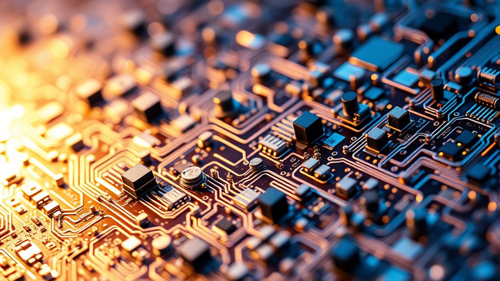
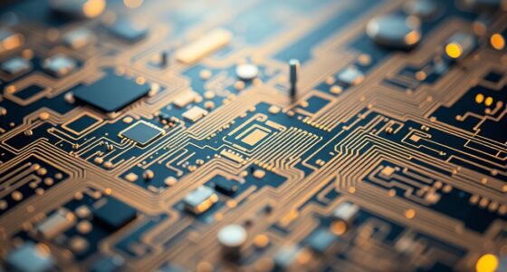
Nanotechnology is revolutionizing the semiconductor industry by enabling the development of smaller, faster, and more energy-efficient chips. One of the key innovations driving this progress involves the use of quantum dots. These tiny semiconductor particles, often just a few nanometers across, have unique optical and electronic properties that traditional materials can’t match. When integrated into semiconductor devices, quantum dots can improve performance by precisely controlling electron behavior at a scale where classical physics no longer applies. They serve as highly tunable light emitters or detectors, making them invaluable for applications like quantum computing, displays, and sensors. As you work with quantum dots, you’ll notice that their size directly influences their energy levels, allowing you to tailor their properties for specific functions. This tunability results in more efficient transistors, better light absorption for photovoltaic cells, and enhanced signal processing capabilities.
However, working with such minuscule particles presents challenges. Quantum dots tend to be unstable or prone to aggregation, which can impair device performance. That’s where surface passivation comes into play. Surface passivation involves coating or treating the quantum dots to stabilize their surface and prevent unwanted reactions. When you apply surface passivation, you’re essentially covering the reactive surface sites with a layer that neutralizes defect states, reduces non-radiative recombination, and enhances the quantum dots’ overall stability. This process is critical because surface defects can trap charge carriers, leading to energy losses and slower device response times. By passivating these defects, you improve the efficiency and lifespan of your semiconductor components. Additionally, advances in nanomaterial engineering are continually refining surface passivation techniques to further boost quantum dot stability and performance.
In addition to stabilizing quantum dots, surface passivation can also modify their interaction with surrounding materials, allowing for more precise integration into complex semiconductor architectures. This means you can better control how quantum dots transfer energy or charge, which directly impacts the performance of your devices. The combination of quantum dots and effective surface passivation techniques open up new levels of miniaturization and energy efficiency. As you explore these nanotech strategies, you’ll find that they open up opportunities for innovation across a wide range of applications—from ultra-efficient solar cells to high-speed computing chips. Embracing these tools lets you push the boundaries of what’s possible in semiconductor technology, making devices smarter, faster, and more sustainable.
Frequently Asked Questions
How Does Nanotech Influence Semiconductor Manufacturing Costs?
Nanotech substantially lowers your semiconductor manufacturing costs by enhancing manufacturing efficiency and enabling cost reduction. It allows you to produce smaller, more powerful chips with less material, speeding up the production process. With nanotech, you can reduce waste and improve precision, which cuts expenses. Overall, integrating nanotech helps you achieve higher yields and faster production, making your semiconductor manufacturing more cost-effective and competitive in the market.
What Are the Environmental Impacts of Nanomaterials in Semiconductors?
You might find that nanomaterials in semiconductors can cause environmental pollution if not properly managed, as they may release toxic particles during production or disposal. Additionally, their use can contribute to resource depletion because sourcing nanomaterials often requires significant energy and raw materials. To minimize these impacts, it’s vital to develop sustainable manufacturing practices and recycling methods that reduce pollution and conserve resources.
Can Nanotech Improve Semiconductor Lifespan and Durability?
Yes, nanotech can markedly improve your semiconductor’s lifespan and durability. By applying advanced nanotech coatings, you enhance semiconductor resilience against wear, corrosion, and thermal stress. These ultra-thin coatings provide a protective barrier, reducing damage from environmental factors and operational stress. As a result, your semiconductors last longer, perform more reliably, and require less maintenance, making nanotech an essential tool for extending device longevity and ensuring consistent performance.
Are There Any Health Risks Associated With Nanotech in Semiconductors?
You should be aware that nanotech in semiconductors does pose some health safety and toxicity concerns. When handling nanomaterials, there’s a risk of inhalation or skin exposure, which could lead to cellular damage or other health issues. Manufacturers are working to minimize these risks through strict safety protocols, but it is crucial to stay informed and use proper protective equipment to avoid potential toxicity concerns associated with nanomaterials.
How Quickly Can Nanotech Innovations Be Integrated Into Existing Semiconductor Tech?
Integration of nanotech innovations into existing semiconductor tech moves like a finely tuned engine, but the timeline depends on your readiness for change. Typically, the integration timeline spans several years, requiring careful technological adaptation. You’ll need to navigate research, development, and testing phases, balancing speed with precision. With strategic planning, you could see nanotech enhancements boosting performance within this timeframe, transforming your semiconductor processes into a sleek, next-generation powerhouse.
Conclusion
By harnessing nanotech, you can substantially boost semiconductor efficiency, much like sharpening a blade to perfection. These tiny innovations act as the secret sauce, making your devices faster and more energy-efficient. As you explore this cutting-edge tech, remember that the future of electronics is as bright as a lighthouse guiding ships through darkness. Embrace nanotechnology, and watch your advancements shine brighter than ever before.