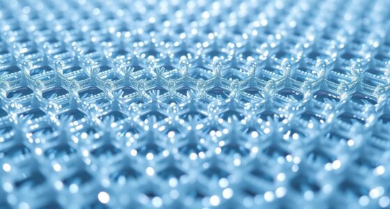

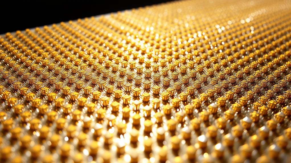
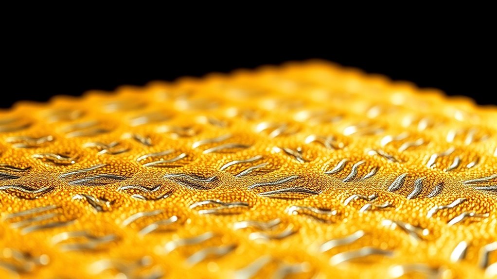
Nanostructured plasmonic solar absorbers use tiny metal structures to trap and intensify sunlight, boosting energy conversion efficiency. These structures excite surface plasmons that enhance light absorption across a broad spectrum, helping you capture more solar power. Materials like silver, gold, or alternatives are crafted through advanced techniques such as nanoimprinting and lithography. If you’re interested, you’ll discover how innovative designs and emerging technologies are shaping the future of high-performance solar devices.
Key Takeaways
- Nanostructured plasmonic absorbers utilize surface plasmons to enhance light trapping and broadband solar spectrum absorption.
- Material choice, such as silver, gold, aluminum, or copper, balances performance, cost, and environmental stability.
- Fabrication techniques like electron beam lithography and nanoimprinting enable precise control of nanostructure geometry for optimal resonance.
- Design strategies include tuning size, shape, and multilayer coatings to maximize spectral absorption and light concentration.
- Challenges involve scalability, durability, and cost-effective manufacturing, with future trends focusing on novel materials and advanced fabrication methods.
Fundamentals of Plasmonic Nanostructures in Solar Energy
Have you ever wondered how nanostructures can enhance solar energy absorption? It all comes down to plasmonic coupling and electron oscillations. When light hits a nanostructure, it excites electrons, causing them to oscillate collectively—these are surface plasmons. This plasmonic coupling amplifies the local electromagnetic field, allowing the nanostructure to trap and concentrate sunlight more efficiently. Unlike bulk materials, these tiny structures can resonate at specific frequencies, boosting absorption across a broader spectrum. By harnessing electron oscillations, plasmonic nanostructures increase the likelihood of photon-to-electron conversion, improving solar device performance. Additionally, the design of nanostructures can be optimized to noise reduction technology, which enhances their stability and efficiency in real-world applications. Understanding these fundamental interactions helps us design better nanostructured absorbers that maximize energy harvesting from sunlight.
Design Principles of Nanostructured Absorbers

To optimize nanostructured absorbers, you need to focus on material selection strategies that maximize plasmonic response while minimizing losses. Geometric resonance tuning allows you to adjust nanostructure dimensions for peak absorption at specific wavelengths. Incorporating multi-scale nanostructures helps you broaden the absorption spectrum and enhance overall efficiency.
Material Selection Strategies
Selecting appropriate materials is essential for designing effective nanostructured plasmonic solar absorbers. You need materials that offer high material durability to withstand environmental conditions and prolonged exposure to sunlight. Choosing materials with excellent stability guarantees your absorber maintains performance over time, reducing maintenance costs. Cost effectiveness is equally important; opt for materials that balance performance with affordability, making large-scale deployment feasible. Common choices include metals like silver and gold, known for their strong plasmonic properties, but their costs can be high. Alternatives such as aluminum or copper can be more economical, though they may have slightly lower performance. Ultimately, your material selection should align with your project’s durability requirements and budget constraints, ensuring an optimal balance between efficiency, longevity, and affordability.
Geometric Resonance Tuning
Designing nanostructured plasmonic solar absorbers involves carefully tuning their geometric features to maximize light absorption. You achieve this through structural tuning, adjusting parameters like size, shape, and spacing to modify the resonance frequency. By fine-tuning these features, you shift the resonance to match the solar spectrum’s most intense regions, enhancing absorption efficiency. Precise control over the geometry allows you to manipulate localized surface plasmon resonances, ensuring they align with desired wavelengths. This process involves iterative design and simulation, where small changes in dimensions result in significant shifts in resonance frequency. Ultimately, structural tuning enables you to optimize the nanostructure’s optical response, making it more effective at capturing and converting incident sunlight into usable energy.
Multi-scale Nanostructures
Implementing multi-scale nanostructures in plasmonic solar absorbers involves integrating features of different sizes and geometries to enhance light trapping across a broad spectrum. This approach leverages quantum effects, such as localized surface plasmon resonances, to improve absorption efficiency. By combining nanoscale features with larger structures, you can increase the interaction of incident light with the absorber, reducing reflection and transmission losses. Additionally, multi-scale designs aid thermal management by dispersing heat more effectively, preventing localized hotspots that degrade performance. This hierarchical structuring enables better control over electromagnetic fields and enhances spectral coverage, making your absorber more versatile. Overall, multi-scale nanostructures optimize light absorption and thermal stability, pushing the efficiency limits of plasmonic solar devices.
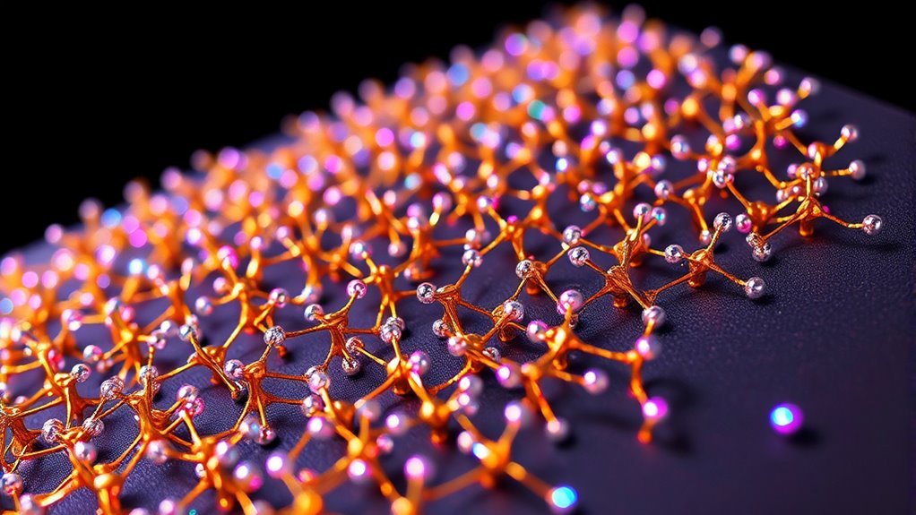
Materials Used in Plasmonic Solar Devices
Materials play a essential role in the performance of plasmonic solar devices, as they directly influence how effectively these systems absorb and convert sunlight. For improved efficiency, researchers explore materials like metals, quantum dots, and hybrid materials that enhance light capture and stability. Metals such as silver and gold support strong surface plasmon resonances, but quantum dots offer tunable absorption spectra, making them promising for multi-junction devices. Hybrid materials combine the best properties of different components, optimizing performance. Consider this table highlighting key materials:
| Material | Advantages | Limitations |
|---|---|---|
| Silver | Strong plasmonic response | Susceptible to corrosion |
| Gold | Chemical stability | Higher cost |
| Quantum dots | Tunable absorption, size control | Potential toxicity |
| Hybrid materials | Customizable, versatile | Complex fabrication |
Additionally, ongoing research aims to develop more durable materials that can withstand environmental stresses while maintaining high efficiency.
Light Absorption and Enhancement Mechanisms
Nanostructured plasmonic materials enhance light absorption by focusing electromagnetic energy into tiny regions, creating intense local fields. This process relies heavily on plasmonic coupling, where surface plasmons on nanostructures interact with incident light, boosting absorption efficiency. Near field effects play a critical role by amplifying electromagnetic fields close to the nanostructure surfaces, enabling better energy transfer into the absorber material. When plasmonic particles are properly arranged, they can trap and concentrate light within subwavelength distances, markedly increasing the optical path length. This synergy between plasmonic coupling and near field effects results in more effective light harvesting, making nanostructured plasmonic absorbers highly efficient in capturing incident solar radiation. These mechanisms are fundamental to optimizing solar cell performance through improved light management. Understanding light management techniques further enhances the design of efficient plasmonic solar absorbers.
Fabrication Techniques for Nanoscale Structures
Creating nanoscale structures for plasmonic solar absorbers involves a variety of advanced fabrication techniques that enable precise control over size, shape, and arrangement. You might use methods like:
- Nanoimprinting techniques, which allow you to create consistent, high-resolution patterns on surfaces by pressing a mold into a resist layer.
- Chemical vapor deposition (CVD), ideal for depositing thin, uniform metal or dielectric films essential for plasmonic effects.
- Electron beam lithography, providing exact patterning at the nanoscale for custom structures.
- Reactive ion etching, which sharpens features or creates complex geometries by selectively removing material.
- Additionally, understanding appliance maintenance plans can inform the development of durable, energy-efficient materials for scalable nanofabrication processes.
These techniques offer versatility and precision, helping you tailor nanostructures to optimize light absorption and enhance solar device performance.
Performance Metrics and Efficiency Improvements

To improve your plasmonic solar absorbers, focus on how well they enhance the absorption spectrum and trap light. Optimizing spectral selectivity can boost efficiency by targeting specific wavelengths. These metrics directly impact the overall performance and viability of your solar technology. Additionally, selecting materials with high efficiency ratings can further maximize energy conversion.
Absorption Spectrum Enhancement
Enhancing the absorption spectrum of plasmonic solar absorbers directly boosts their efficiency by capturing a broader range of sunlight. You can achieve this through several strategies:
- Tuning nanostructure size and shape to target specific wavelengths, maximizing quantum effects for improved absorption.
- Incorporating materials with high thermal stability to ensure consistent performance under intense sunlight.
- Using multilayer designs to extend absorption into the near-infrared region, capturing more energy.
- Employing dielectric coatings to modify local electromagnetic fields, boosting absorption without sacrificing stability. These approaches help optimize performance metrics while maintaining thermal stability. By broadening the spectrum, you can considerably improve overall efficiency, making your plasmonic absorbers more effective in real-world conditions.
Light Trapping Efficiency
Optimizing light trapping efficiency is essential for maximizing the performance of plasmonic solar absorbers. You achieve this by enhancing plasmonic coupling, which strengthens interactions between incident light and nanostructures, leading to increased absorption. Light scattering plays a pivotal role by redirecting photons into the active layer, extending their path length and boosting absorption probability. By carefully designing nanostructures, you can control scattering angles and intensities, improving overall light trapping. Incorporating metallic nanostructures that support localized surface plasmon resonances further amplifies scattering effects. These strategies work together to reduce reflection losses and increase the amount of light captured. As a result, your solar device’s efficiency improves, making it more effective at converting sunlight into usable electrical energy through optimized light trapping.
Spectral Selectivity Optimization
Spectral selectivity plays a essential role in improving the overall efficiency of plasmonic solar absorbers by tailoring their response to specific wavelengths of sunlight. To optimize this, you can focus on key strategies:
- Enhance plasmonic coupling to concentrate absorption at targeted wavelengths, boosting spectral filtering effectiveness.
- Design nanostructures that selectively absorb visible or infrared light, reducing energy losses.
- Use multilayer coatings to sharpen spectral response and improve selectivity.
- Incorporate tunable plasmonic materials to dynamically adjust spectral filtering based on sunlight conditions.
These approaches maximize light absorption where it’s most efficient, minimizing unwanted spectral contributions and increasing overall device performance. Precise spectral selectivity enables higher conversion efficiencies and better integration into solar energy systems.
Challenges and Limitations in Development

Despite the promising potential of nanostructured plasmonic solar absorbers, several challenges hinder their widespread implementation. Scalability issues pose a significant barrier, as fabricating complex nanostructures consistently at large scales remains difficult and costly. Achieving uniformity across large areas is critical for practical applications, yet current techniques often fall short. Environmental stability also presents concerns; nanostructured materials can degrade when exposed to moisture, UV radiation, and temperature fluctuations, reducing their efficiency over time. Developing robust, long-lasting materials requires overcoming these stability challenges without compromising optical performance. Additionally, understanding resources and tools available for optimizing design and fabrication processes can facilitate overcoming these obstacles. Addressing scalability and environmental stability is essential for progressing from laboratory prototypes to commercial solar devices, ensuring your advancements are both feasible and sustainable in real-world settings.
Future Directions and Emerging Trends
Emerging trends in nanostructured plasmonic solar absorbers focus on integrating novel materials and advanced fabrication techniques to overcome current limitations. You’ll see efforts to harness quantum effects, which can enhance light absorption and carrier dynamics at the nanoscale. Improving environmental stability is also key, ensuring long-term performance in real-world conditions. Specifically, you should watch for:
- Incorporation of hybrid materials that combine metals with dielectrics for better durability.
- Development of scalable, cost-effective fabrication methods for complex nanostructures.
- Exploration of quantum effects to boost efficiency beyond classical limits.
- Strategies to enhance environmental stability, preventing degradation from moisture, heat, and UV exposure.
- Advances in Kia Tuning technology may inspire innovative approaches to optimize nanostructure design for solar applications.
These trends aim to push the boundaries of efficiency, durability, and practical application of plasmonic solar absorbers.
Frequently Asked Questions
How Do Nanostructures Affect the Durability of Solar Absorbers?
Nanostructures can improve your solar absorber’s durability by reducing nanostructure degradation and material corrosion. They create protective layers that shield against environmental factors, preventing corrosion and physical wear. However, if not properly designed, nanostructures may accelerate degradation or weaken the material. You should carefully select materials and coatings to guarantee long-term stability, balancing enhanced performance with resistance to environmental stressors.
What Are the Cost Implications of Large-Scale Production?
You’ll find that large-scale production of nanostructured plasmonic solar absorbers can lower manufacturing costs due to material scalability and process efficiencies. However, initial investments in specialized equipment and high-quality materials may increase upfront expenses. As production scales up, these costs tend to decrease, making the technology more economically viable. Overall, balancing material costs and scalability is key to reducing long-term expenses and expanding commercial adoption.
Can Nanostructured Plasmonic Absorbers Be Integrated With Existing Solar Technologies?
You can definitely integrate nanostructured plasmonic absorbers with existing solar technologies through hybrid integration. While fabrication challenges exist, advancements in nanofabrication techniques are making it increasingly feasible. Remember, “a chain is only as strong as its weakest link,” so addressing these challenges guarantees seamless integration. This combination can boost efficiency, making solar power more versatile and effective without overhauling current systems.
How Do Environmental Factors Influence Nanostructure Stability?
Environmental factors like temperature fluctuations, humidity, and exposure to chemicals can considerably impact nanostructure stability. These conditions may cause environmental degradation, leading to corrosion or oxidation that weakens the nanostructures. To guarantee long-term efficiency, you need to focus on enhancing chemical stability through protective coatings and selecting materials resistant to environmental stresses. Proper encapsulation and environmental controls can help maintain nanostructure integrity over time.
Are There Any Safety Concerns Associated With Nanomaterials in Solar Devices?
Think of nanomaterials in solar devices as tiny, powerful explorers. While they boost efficiency, nanoparticle toxicity raises safety concerns, much like hidden dangers lurking in a quest. Regulatory concerns also emerge, requiring careful oversight. You should handle these materials with caution, ensuring proper disposal and safety measures. Ongoing research aims to minimize risks, but staying informed helps protect both you and the environment from potential hazards.
Conclusion
Think of nanostructured plasmonic absorbers as the lighthouse guiding solar energy to its full potential. Their intricate designs and materials act as the beacon, amplifying light like a lighthouse beam cuts through darkness. While challenges remain, your innovation can turn these nanoscale marvels into powerful engines of clean energy. Embrace the symbolism of light and hope—each breakthrough brings us closer to a sustainable future illuminated by the tiny yet mighty nanostructures.