

Nanotechnology advances enable you to manufacture flexible electronics with lightweight, durable, and high-performance features. By using nanomaterials like graphene and carbon nanotubes, you can achieve better electrical conductivity, mechanical flexibility, and heat management. Precise nanoscale fabrication techniques, such as lithography and self-assembly, help create intricate patterns for large-area devices. Employing these methods improves device lifespan, responsiveness, and thermal stability. Keep exploring how nanotech transforms the future of flexible electronics and their applications.
Key Takeaways
- Nanomaterials enable precise patterning and scalable fabrication of flexible electronic components via techniques like lithography and self-assembly.
- Incorporation of nanostructures enhances electrical conductivity, device responsiveness, and thermal management in flexible electronics.
- Nanoscale patterning methods, such as nanoimprint lithography and electron beam patterning, facilitate high-resolution, large-area manufacturing.
- Self-assembly processes enable cost-effective and uniform formation of nanostructures, improving device durability and performance.
- Addressing manufacturing scalability and safety regulations is crucial for integrating nanotechnology into flexible electronics production.
2D Nanomaterials and Devices for Flexible Electronics
As an affiliate, we earn on qualifying purchases.
As an affiliate, we earn on qualifying purchases.
The Role of Nanomaterials in Flexible Electronics

Nanomaterials play a essential role in advancing flexible electronics by providing unique properties that bulk materials cannot achieve. Their small size grants enhanced electrical conductivity, mechanical flexibility, and lightweight characteristics, making them ideal for bendable devices. However, you should also consider nanomaterial toxicity and environmental impact. Some nanomaterials, like certain metal oxides or carbon-based nanoparticles, can pose health risks if not handled properly. Additionally, their environmental footprint during manufacturing and disposal raises concerns about pollution and ecological harm. As you develop flexible electronic components, balancing performance benefits with safety and sustainability is indispensable. Proper assessment of nanomaterial toxicity and a focus on eco-friendly practices will ensure these innovations are both effective and responsible. Law of Attraction Resources can offer insights into sustainable and positive development practices for new technologies.

Conductive PU Film Carbon nanotube Graphene Film electrically Heated Therapy Electrode Patch Anti-Static Pressure Sensitive Conductive (400 x 400 mm)
Conductive body: conductive carbon black/multi walled carbon nanotubes; Thickness 0.03-0.1mm; Weight 10-50g/m2; Far infrared emissivity 80-90%; Square resistance…
As an affiliate, we earn on qualifying purchases.
As an affiliate, we earn on qualifying purchases.
Fabrication Techniques at the Nanoscale

You need precise control over nanoscale features, which is achieved through techniques like lithography and patterning. Self-assembly processes allow nanostructures to form naturally, reducing fabrication complexity. Direct nanoscale writing offers flexibility by allowing you to create custom patterns with high accuracy. Additionally, understanding sound healing science can inspire innovative approaches to improving fabrication environments through specific frequencies and vibrations.
Lithography and Patterning
Lithography and patterning are fundamental techniques in fabricating nanoscale features essential for flexible electronics. These methods enable precise control over tiny structures critical for device performance. Nanoimprint lithography offers high-resolution pattern transfer by pressing a mold into a resist, making it ideal for large-area production. Electron beam patterning uses a focused electron beam to directly write intricate designs, achieving exceptional detail. Both techniques allow you to create complex nanoscale patterns essential for flexible circuits and sensors.
| Technique | Advantage | Limitation |
|---|---|---|
| Nanoimprint lithography | Fast, suitable for high volume | Mold fabrication complexity |
| Electron beam patterning | Ultra-high resolution | Slower, more expensive |
| Both | Precise nanoscale control | Equipment cost |
Self-Assembly Processes
Self-assembly processes harness the natural tendency of molecules and nanoparticles to organize into well-defined structures without extensive external intervention. Using self assembly techniques, you can create complex nanoscale patterns by simply allowing materials to spontaneously organize through chemical and physical interactions. This spontaneous organization relies on forces like van der Waals, electrostatic, or hydrophobic interactions, guiding particles into precise arrangements. These processes enable you to fabricate uniform thin films, nanowires, and ordered arrays with minimal effort and high precision. By controlling parameters such as temperature, concentration, and surface chemistry, you influence the self-assembly outcome. This approach offers a scalable, cost-effective alternative to traditional lithography, making it ideal for flexible electronics where large-area, nanoscale patterning is essential.
Direct Nanoscale Writing
Direct nanoscale writing involves precisely manipulating materials at the atomic or molecular level to create detailed patterns and structures. This technique allows you to craft intricate features with high accuracy, essential for flexible electronics. You can use methods like nano pen techniques, where a fine tip deposits or etches material directly onto a substrate, or tip-based lithography, which patterns surfaces with nanoscale precision. These approaches enable rapid prototyping and custom designs without complex masks.
- You achieve precise control over pattern dimensions.
- You can rapidly modify designs at the nanoscale.
- You facilitate the integration of complex, flexible electronic components.
nanoimprint lithography kit
As an affiliate, we earn on qualifying purchases.
As an affiliate, we earn on qualifying purchases.
Enhancing Electrical Performance With Nanotechnology

By integrating conductive nanomaterials, you can substantially boost the electrical performance of flexible electronics. These materials enhance electron mobility, allowing devices to operate more efficiently. As a result, your designs benefit from improved conductivity and faster response times. Incorporating electric power generation techniques with nanotechnology can further optimize energy efficiency in flexible devices.
Conductive Nanomaterials Integration
Integrating conductive nanomaterials into flexible electronic systems markedly boosts their electrical performance. You can enhance device sensitivity, reduce power consumption, and improve signal stability by incorporating materials like graphene sensors and quantum dots. Graphene sensors offer exceptional conductivity and flexibility, making them ideal for detecting chemical or biological signals in wearables. Quantum dots contribute unique optoelectronic properties, enabling better light absorption and emission. To maximize benefits, consider these key points:
- Select nanomaterials with high conductivity and compatibility with flexible substrates.
- Optimize the dispersion and alignment of nanomaterials for uniform electrical pathways.
- Utilize hybrid approaches, combining materials like graphene and quantum dots, for multifunctionality.
This integration leads to more responsive, reliable, and innovative flexible devices.
Improved Electron Mobility
Nanotechnology considerably boosts electron mobility in flexible electronic devices, leading to faster response times and lower power consumption. By reducing electron scattering through nanoscale engineering, you can enhance charge transport efficiency. Nanomaterials enable smoother pathways for electrons, minimizing resistance. Quantum tunneling effects become significant at this scale, allowing electrons to pass through barriers more easily, further improving mobility.
| Technique | Benefit |
|---|---|
| Nanoscale material design | Reduces electron scattering |
| Thin-layer engineering | Enhances quantum tunneling efficiency |
| Surface passivation | Minimizes electron trapping |
These strategies collectively improve electrical performance, making flexible electronics more responsive and energy-efficient. Understanding quantum tunneling and electron scattering helps you optimize nanotech solutions for superior electron mobility.
electron beam patterning equipment
As an affiliate, we earn on qualifying purchases.
As an affiliate, we earn on qualifying purchases.
Mechanical Flexibility and Durability Improvements
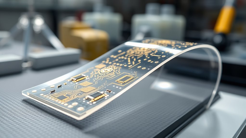
Advancements in nanotechnology have considerably enhanced the mechanical flexibility and durability of materials used in flexible electronics. These improvements boost stress resistance and bend endurance, making devices more resilient during repeated use. To achieve this, researchers focus on several key strategies:
- Incorporating nanomaterials like graphene and carbon nanotubes to distribute stress evenly across the device.
- Developing flexible substrates that can withstand repeated bending without cracking.
- Engineering nanostructures that absorb strain, preventing damage during flexing.
- Optimizing color accuracy in the materials to ensure consistent visual performance even under mechanical stress.
These innovations allow your devices to endure daily flexing and stretching without compromising performance. As a result, flexible electronics become more reliable, long-lasting, and better suited for real-world applications where mechanical stress is unavoidable.
Thermal Management in Nano-Enabled Devices

As flexible electronic devices become more complex, managing heat effectively is crucial to maintaining performance and longevity. Nano-enabled materials can markedly improve heat dissipation by enhancing thermal conductivity. Incorporating nanostructures like graphene or carbon nanotubes allows you to create highly efficient thermal pathways, which spread heat quickly and prevent hotspots. This is especially important for maintaining device stability during operation. You can design flexible substrates with embedded nanomaterials to optimize thermal management without sacrificing flexibility. By improving thermal conductivity at the nanoscale, you reduce the risk of overheating, extend device lifespan, and ensure consistent performance. Effective thermal management using nanotechnology is indispensable for advancing flexible electronics into more demanding applications. Understanding thermal properties at the nanoscale is essential for developing innovative solutions in this field.
Applications and Innovations Driven by Nanotech

Innovations in nanotechnology are transforming flexible electronics by enabling new functionalities and enhancing performance. Quantum dots, for example, improve display brightness and color accuracy, making screens more vivid and energy-efficient. Nano sensors are now integrated into devices to monitor environmental conditions, health metrics, and device integrity in real-time. These advancements lead to smarter, more responsive products. Consider these key innovations: 1. Quantum dots enable high-resolution, energy-efficient displays with richer colors. 2. Nano sensors facilitate real-time data collection, improving device adaptability. 3. Nanomaterials enhance flexibility, durability, and overall device lifespan. Understanding nanomaterials is crucial for appreciating how these improvements are achieved.
Future Perspectives and Challenges in Nano-Flexible Electronics
While nanotechnology offers exciting possibilities for flexible electronics, realizing its full potential requires overcoming significant challenges. Scalability hurdles remain a major obstacle, as manufacturing processes that work on a small scale often struggle to be cost-effective and reliable at industrial levels. You’ll need to develop new fabrication techniques that can produce consistent, high-quality nanomaterials at larger volumes. Additionally, regulatory considerations pose a critical challenge, as the safety and environmental impacts of nanomaterials are still under evaluation. You must navigate evolving standards and policies to ensure compliance without stifling innovation. Addressing these issues demands collaboration between researchers, industry leaders, and policymakers. By tackling scalability hurdles and regulatory concerns, you can help shape a future where nano-flexible electronics become widespread, safe, and commercially viable. Moreover, fostering creative practice in research can lead to innovative solutions for these complex challenges.
Frequently Asked Questions
What Environmental Impacts Are Associated With Nanomaterials in Flexible Electronics?
You should be aware that nanomaterials in flexible electronics can pose environmental risks, including environmental toxicity and resource depletion. These tiny particles may harm ecosystems if released, and their production often consumes significant resources, contributing to environmental strain. You need to contemplate proper disposal and sustainable manufacturing practices to minimize these impacts, ensuring that the benefits of nanotechnology don’t come at the expense of environmental health.
How Cost-Effective Are Nanotechnology-Based Manufacturing Processes for Large-Scale Production?
You’ll find that nanotechnology-based manufacturing processes can be quite cost-effective for large-scale production. They enable significant cost reduction by improving material efficiency and reducing waste. Additionally, these processes enhance production scalability, allowing you to ramp up manufacturing quickly without sacrificing quality. As a result, adopting nanotech methods can make flexible electronics more affordable, helping you meet market demands efficiently while maintaining high performance standards.
Are There Any Health Risks Linked to Nanomaterials Used in Flexible Devices?
You should be aware that nanomaterials used in flexible devices can pose health risks, especially concerning material toxicity. Workers handling these nanomaterials need proper safety protocols to minimize exposure and protect their health. While research continues, current evidence suggests potential risks like respiratory or skin issues. Ensuring strict safety measures and ongoing monitoring helps reduce health hazards linked to nanotechnology in manufacturing environments.
How Do Nanomaterials Influence the Recyclability of Flexible Electronic Components?
Nanomaterials can present recycling challenges due to their unique properties, which sometimes lead to nanomaterial degradation during disassembly. This makes reclaiming and reusing components more difficult, potentially complicating sustainable practices. While they enhance device performance, their influence on recyclability requires careful consideration, as the tiny structures may hinder traditional recycling methods. To improve sustainability, developing innovative recycling techniques for nanomaterial-based components is essential.
What Regulatory Frameworks Govern the Use of Nanotechnology in Consumer Electronics?
You need to understand that regulatory standards govern nanotechnology in consumer electronics, ensuring safety and environmental protection. Agencies like the EPA and FDA set guidelines you must follow. Patent considerations are also vital; protecting your innovations is essential for market success. Staying compliant with these frameworks helps you avoid legal issues, promotes responsible use, and fosters consumer trust in your nanotech-enabled flexible electronics.
Conclusion
So, now you’re all set to revolutionize flexible electronics with nanotech—because, obviously, tiny materials will solve every bendy gadget problem out there. Who needs bulky components or old-fashioned manufacturing methods when you can just sprinkle some nanomagic? Just remember, as you embark on this nanoscale wonderland, don’t forget to bring your patience—after all, working at the smallest scale might just be the biggest challenge of all. Happy nano-engineering!