
Conductive inks with nanomaterials let you create flexible, high-performance circuits on various surfaces like plastics and textiles. By combining optimized formulations with well-synthesized nanoparticles, you can achieve low resistivity, durable, and bendable printed electronics. Proper dispersion and stability of nanoparticles are key to consistent conductivity and adhesion. Mastering these techniques opens up new possibilities in flexible displays, wearable devices, and sensors—if you stay curious, you’ll discover even more about their potential.
Key Takeaways
- Conductive inks utilize nanoparticles like silver, copper, and gold to achieve high electrical conductivity in printed electronics.
- Precise nanoparticle synthesis controls size, shape, and purity, enhancing ink performance and conductivity.
- Proper dispersion and stabilization of nanoparticles in inks prevent aggregation, ensuring consistent electrical properties.
- Formulating conductive inks involves optimizing viscosity, surface tension, and drying time for durable, flexible printed circuits.
- Combining advanced nanoparticle synthesis with tailored ink formulations enables applications in flexible displays, wearables, and sensors.

Have you ever wondered how flexible electronics and printed circuits achieve their remarkable conductivity? The secret lies in the development of advanced conductive inks, which rely heavily on meticulous ink formulation and sophisticated nanoparticle synthesis. These components work together to produce inks that are not only highly conductive but also adaptable to various substrates, making them ideal for modern electronic applications.
Advanced conductive inks combine precise formulation and nanoparticle synthesis for flexible, high-performance electronic applications.
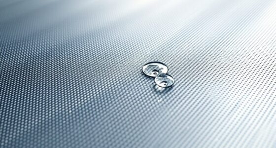
The process begins with ink formulation, where you select the right mixture of solvents, binders, and conductive materials. The goal is to create an ink that flows smoothly during printing but also forms a stable, conductive film once dried or cured. Achieving this balance requires understanding how different ingredients interact. For instance, the viscosity must be just right to guarantee precise deposition, while the surface tension influences how well the ink adheres to the substrate. Formulation also involves controlling the ink’s drying time and flexibility, especially for applications on flexible plastics or textiles. The right formulation assures that the printed circuits maintain their conductivity even when bent or stretched.
Nanoparticle synthesis plays a critical role in enhancing the electrical performance of conductive inks. You generate nanoparticles, such as silver, copper, or gold, through controlled synthesis methods that produce particles with uniform size and shape. Smaller, evenly sized nanoparticles create a larger surface area, which substantially improves the ink’s ability to conduct electricity. Synthesis techniques like chemical reduction, sol-gel processes, or thermal decomposition allow you to produce these particles with high purity and tailored properties. Once synthesized, nanoparticles are dispersed into the ink’s carrier solution, where their stability and dispersion quality become crucial. Proper dispersion prevents aggregation, securing consistent conductivity and printing quality.
The synergy between ink formulation and nanoparticle synthesis ultimately determines the effectiveness of the conductive ink. When nanoparticles are well-synthesized and evenly distributed, the ink exhibits low resistivity and excellent adhesion. You can then print these inks onto a variety of surfaces, from flexible plastic films to paper, creating circuits that are both durable and conductive. This combination of precise formulation and nanoparticle engineering unlocks new possibilities in flexible displays, wearable electronics, and printed sensors.
In essence, understanding the intricacies of ink formulation and nanoparticle synthesis empowers you to develop superior conductive inks that push the boundaries of modern electronics. It’s a delicate balance—one that requires careful control at each step—but the payoff is a material capable of transforming how we design and manufacture electronic devices.
Top picks for "conductive inks nanomaterial"
Open Amazon search results for this keyword.
As an affiliate, we earn on qualifying purchases.
Frequently Asked Questions
How Do Conductive Inks Compare in Cost to Traditional Conductive Materials?
You’ll find that conductive inks are generally more cost-effective compared to traditional conductive materials. Their material affordability makes them an attractive choice for many applications, especially in large-scale or flexible electronics. While traditional materials might have higher initial costs, conductive inks offer easier processing and lower overall expenses. This cost comparison helps you save money without sacrificing performance, making them a practical option for various innovative projects.
What Are the Environmental Impacts of Producing Nanomaterials for Inks?
Producing nanomaterials for inks can release environmental pollution the size of a city and drain resources faster than a raging wildfire. You might not see it happening, but resource depletion and toxic waste threaten ecosystems and communities. The process often involves hazardous chemicals and energy-intensive steps, making it a significant environmental challenge. If you’re concerned about sustainability, this rapid depletion and pollution should make you think twice.
How Long Do Nanomaterial-Based Conductive Inks Retain Their Conductivity?
Nanomaterial-based conductive inks generally maintain their conductivity for several months to years, depending on their formulation and application. You should consider nanomaterial stability, as factors like environmental exposure, mechanical stress, and ink composition influence the conductive lifespan. Proper storage and protective coatings can extend their durability, ensuring your conductive inks remain effective over time. Regular testing helps monitor their longevity, so you can plan replacements proactively.
Are There Health Risks Associated With Handling Nanomaterials in Inks?
Like Pandora’s box, handling nanomaterials in inks can pose health risks if you’re not careful. You might be exposed to nanoparticles, which could cause respiratory or skin issues. To stay safe, follow strict ink safety protocols, wear protective gear, and work in well-ventilated areas. By taking these precautions, you diminish nanoparticle exposure and ensure your safety while working with these innovative materials.
Can Conductive Inks Be Recycled or Reused in Electronic Devices?
You can recycle and reuse conductive inks in electronic devices, but recycling challenges exist due to their chemical composition and integration with substrates. To overcome this, you might consider reuse methods like removing or reapplying the ink layer or repurposing components. These approaches help reduce waste, but they require specialized processes to guarantee the integrity of the conductive properties and proper recycling of materials.
Conclusion
Just like Icarus reaching for the sun, your innovations with conductive inks and nanomaterials aim high. With these cutting-edge materials, you’re shaping a future where electronics become more flexible, efficient, and sustainable. Remember, even Daedalus’s wings needed careful craftsmanship—so too does mastering these advanced technologies. Keep pushing boundaries, and you’ll find yourself soaring into new domains of possibility, transforming the way we connect and innovate in this electrifying world.