
Nanolattices are innovative 3D architected materials designed at the nanoscale to deliver exceptional strength while remaining lightweight. By precisely manipulating geometric patterns like lattices and hierarchical structures, these materials distribute stress evenly and optimize performance. Advanced manufacturing techniques, such as nano-printing and lithography, enable their creation. Their remarkable strength-to-weight ratios and energy absorption capabilities are revolutionizing industries from aerospace to medicine. To discover how these materials are reshaping the future, explore further details ahead.
Key Takeaways
- Nanoscale lattices utilize precise 3D architectures to maximize strength-to-weight ratios and enhance mechanical performance.
- Advanced manufacturing methods like two-photon lithography enable the fabrication of complex, high-strength nanoscale lattice structures.
- Hierarchical design and geometric repetition distribute stress evenly, preventing failure points and improving durability.
- These materials exhibit exceptional energy absorption, impact resistance, and stiffness while maintaining low weight.
- Such architected nanolattices are transforming industries like aerospace, automotive, and energy storage by offering lightweight, high-strength solutions.
nano 3D lattice materials
As an affiliate, we earn on qualifying purchases.
As an affiliate, we earn on qualifying purchases.
The Principles Behind Nanoscale Architecture
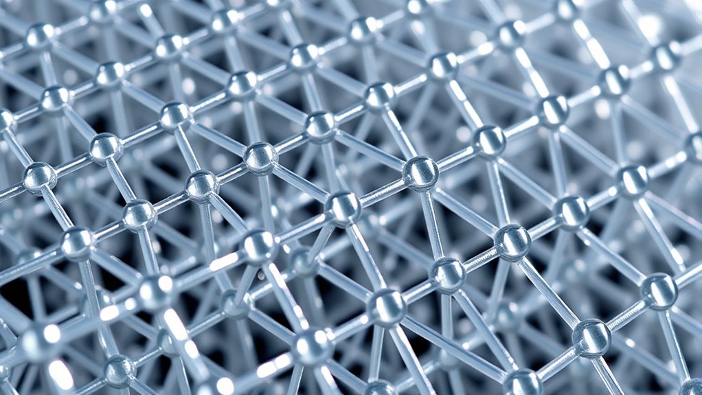
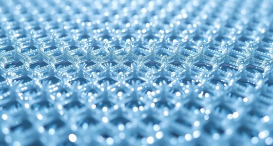
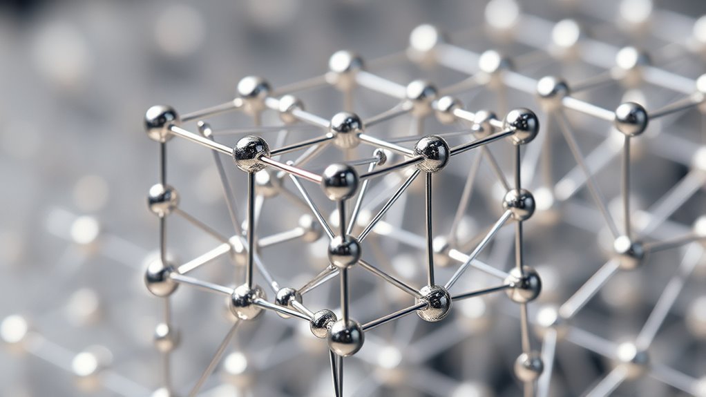
Have you ever wondered how tiny structures can be designed to be both incredibly strong and lightweight? The key lies in understanding nanoscale architecture principles. At this scale, materials don’t rely solely on their chemical composition but on their geometric arrangements. By creating intricate, repeating patterns—like lattices—you can optimize strength-to-weight ratios. These structures distribute stress evenly, preventing failure points. The principles involve manipulating the size, shape, and connectivity of the tiny building blocks to maximize stability without adding weight. This approach mimics natural designs, such as bone and spider silk, which achieve remarkable strength with minimal material. Mastering these principles allows scientists to engineer materials that are both lightweight and durable, pushing the boundaries of what’s possible at the nanoscale.
high strength lightweight nanolattice
As an affiliate, we earn on qualifying purchases.
As an affiliate, we earn on qualifying purchases.
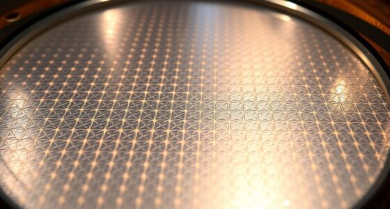
Manufacturing Techniques for Nanoscale Lattices
Creating nanoscale lattices requires advanced manufacturing techniques that can precisely manipulate materials at an atomic or molecular level. Techniques like two-photon lithography, atomic layer deposition, and focused ion beam milling enable you to build intricate, highly controlled structures. These methods allow for the creation of complex geometries with nanoscale accuracy, pushing the boundaries of material science.
nanoscale lattice manufacturing kit
As an affiliate, we earn on qualifying purchases.
As an affiliate, we earn on qualifying purchases.
Mechanical Properties and Performance Advantages

The advanced manufacturing techniques used to build nanoscale lattices directly influence their mechanical properties, enabling remarkable performance characteristics. These structures exhibit exceptional strength-to-weight ratios, often surpassing traditional materials due to their precise architecture and nanoscale features. You’ll find that nanolattices can absorb energy efficiently, providing excellent impact resistance and toughness. Their high specific strength makes them ideal for lightweight applications where durability is vital. Additionally, their hierarchical design allows for tailored deformation behaviors, such as elastic rebound and controlled failure modes. Because of their small size and intricate geometry, nanolattices also demonstrate enhanced stiffness and reduced weight without sacrificing strength. Material optimization plays a crucial role in designing nanolattices to maximize their performance advantages. These performance benefits open doors to innovative uses where maximizing strength, reducing weight, and maintaining resilience are essential.
advanced nanolithography tools
As an affiliate, we earn on qualifying purchases.
As an affiliate, we earn on qualifying purchases.
Applications Transforming Industries

Nanolattices are revolutionizing industries by enabling the development of lighter, stronger, and more resilient materials. In aerospace, they reduce weight without sacrificing strength, improving fuel efficiency and payload capacity. Automotive manufacturers use nanolattices to create crash-resistant, lightweight components that enhance safety and performance. In the energy sector, these materials improve battery durability and efficiency, supporting longer-lasting energy storage. Medical device producers leverage nanolattices to develop implants with superior strength and biocompatibility, reducing failure rates. Sports equipment manufacturers incorporate nanolattices to craft gear that’s both lightweight and highly durable. Overall, nanolattices open new possibilities across sectors, allowing you to design products that are stronger, lighter, and more efficient, transforming how industries approach material performance and innovation. Biodiversity can also be impacted by the environmental effects of manufacturing processes, emphasizing the importance of sustainable development.
Future Directions in Nanoscale Material Design

As research advances, the future of nanoscale material design is poised to unseal even more innovative applications, driven by the integration of artificial intelligence, machine learning, and advanced fabrication techniques. You’ll see smarter algorithms optimize lattice architectures for specific properties, reducing trial-and-error. Precision manufacturing methods like 3D nano-printing will enable you to create complex, tailored nanostructures with unparalleled accuracy. Additionally, hybrid approaches combining biological inspiration with synthetic design will lead to materials that adapt dynamically to their environment. You’ll also harness real-time data to iteratively improve material performance, pushing the boundaries of strength, flexibility, and functionality. Embracing a creative practice mindset will inspire novel solutions and accelerate breakthroughs in nanoscale material development. This synergy of technologies promises a new era of highly customized, efficient nanoscale materials that could revolutionize industries from aerospace to biomedicine.
Frequently Asked Questions
How Do Nanoscale Lattices Compare to Traditional Bulk Materials?
Nanoscale lattices are stronger and lighter than traditional bulk materials because their design allows for efficient load distribution and reduced weight. You’ll find that their architecture enables higher strength-to-weight ratios and improved toughness. Unlike bulk materials, they can be tailored at the nanoscale to optimize properties for specific applications. This makes them ideal for advanced engineering, where maximizing strength while minimizing weight is essential.
What Are the Environmental Impacts of Manufacturing Nanoscale Lattice Structures?
You should be aware that manufacturing nanoscale lattice structures can have environmental impacts, including energy consumption and waste generation from advanced fabrication processes like 3D printing and chemical synthesis. These methods may involve hazardous materials or produce emissions. However, their high strength-to-weight ratio can reduce material usage overall. To minimize environmental impacts, you can focus on sustainable practices, recycling, and developing greener fabrication technologies as industry standards evolve.
Can Nanoscale Architectures Be Recycled or Repurposed Effectively?
Yes, nanoscale architectures can be recycled or repurposed, but it’s challenging. You need specialized techniques to disassemble or reclaim the materials without damaging their intricate structures. If you use biodegradable or environmentally friendly materials, recycling becomes easier. Advances in chemical recycling and reprocessing methods are making it more feasible. Ultimately, with innovation and proper processes, you can improve the sustainability of nanoscale architectures and reduce waste.
What Are the Limitations of Current Nanoscale Fabrication Methods?
You face limitations like high costs, slow production rates, and difficulty achieving precise control at the nanoscale. Current fabrication methods often struggle with scalability and reproducibility, making large-scale production challenging. Techniques such as electron-beam lithography and chemical vapor deposition require expensive equipment and time-consuming processes. Additionally, maintaining structural integrity during fabrication can be tough, restricting the complexity and size of nanostructures you can reliably produce.
How Do Nanoscale Lattice Properties Change Under Extreme Temperatures?
You might find that at extreme temperatures, nanoscale lattice properties subtly shift, becoming less predictable. As temperature rises, atomic vibrations increase, slightly weakening bonds and reducing strength. Nonetheless, with careful material design, you can often mitigate these effects. It’s important to recognize that while high temperatures challenge lattice stability, innovative engineering approaches enable your nanolattices to maintain impressive performance even under harsh conditions.
Conclusion
As you explore nanolattices, you’ll notice how their intricate design unlocks strength at tiny scales, transforming industries in unexpected ways. It’s remarkable how the principles of nanoscale architecture align with manufacturing advances, pushing the boundaries of what’s possible. This convergence of innovation and precision hints at a future where materials aren’t just stronger—they’re smarter, lighter, and more adaptable. In this dance of science and ingenuity, nanolattices reveal that sometimes, the smallest details make the biggest difference.