
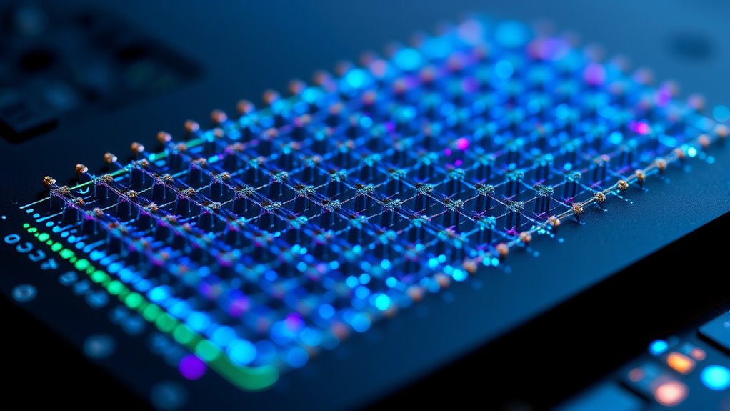
Nanophotonic devices enable you to manipulate light at extremely small scales, using structures like photonic crystals, plasmonic materials, and metasurfaces. These devices control light paths, confine photons, and enhance interactions for applications in communications, sensing, and imaging. Advances in fabrication techniques allow for precise, scalable production of tiny components that improve signal quality and device performance. Keep exploring to discover how these innovations are shaping future technologies at the nanoscale.
Key Takeaways
- Nanophotonic devices control and manipulate light at scales smaller than its wavelength, enabling advanced optical functionalities.
- They utilize structures like photonic crystals, plasmonic materials, and metasurfaces to guide, focus, and steer light precisely.
- Fabrication techniques such as electron beam lithography and self-assembly enable the creation of high-precision nanoscale photonic components.
- These devices enhance optical performance for applications in sensing, imaging, telecommunications, and quantum technologies.
- Challenges include managing losses, scalable manufacturing, and integrating nanophotonic devices with existing electronic systems.
The Fundamentals of Nanophotonics

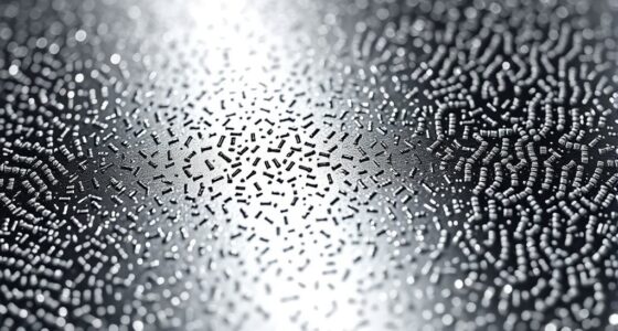
Have you ever wondered how light behaves when it interacts with structures smaller than its wavelength? When light encounters these tiny structures, it doesn’t just pass through or bounce off like it does with larger objects. Instead, it exhibits unique behaviors, such as scattering, confinement, and resonances. These phenomena occur because, at the nanoscale, light interacts strongly with matter, leading to effects like enhanced electromagnetic fields and localized energy. Nanophotonics harnesses these interactions to control and manipulate light in ways traditional optics can’t achieve. By understanding the fundamental principles—like how electromagnetic waves behave at these small scales—you can see how nanophotonics opens the door to innovative devices for sensing, imaging, and communication. It’s all about mastering light’s interactions at the smallest dimensions.
Types of Nanophotonic Structures and Materials
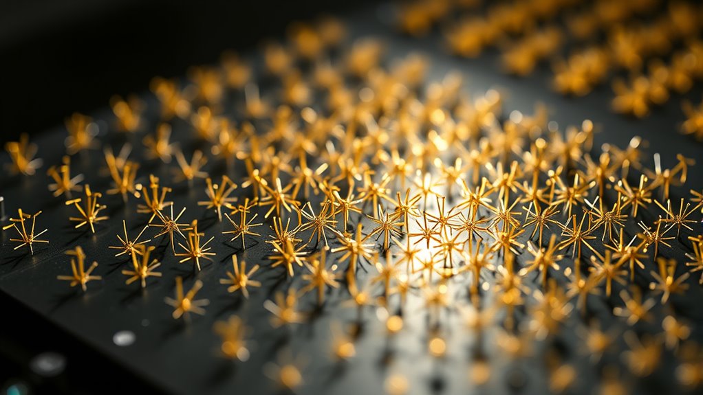
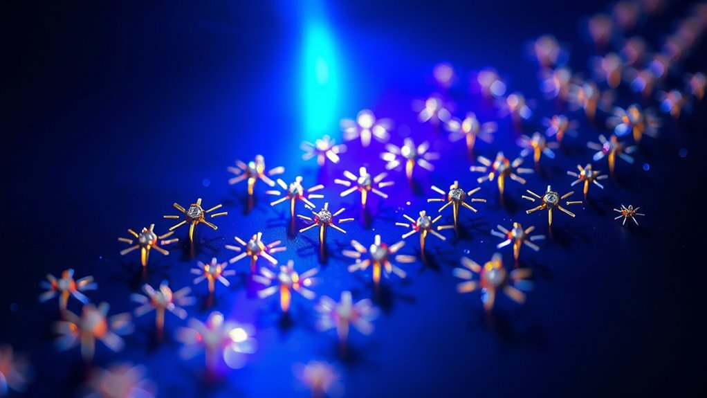
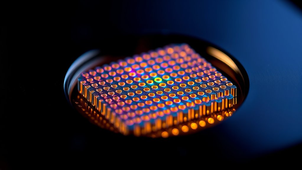
Nanophotonic structures and materials come in a variety of forms, each designed to manipulate light at the nanoscale effectively. You’ll encounter photonic crystals, which control light through periodic dielectric structures that create band gaps. Plasmonic materials, often metals like gold and silver, harness surface plasmon resonances to concentrate light beyond diffraction limits. Dielectric nanoparticles, such as silicon or titanium dioxide, are used for low-loss light manipulation and enhanced scattering. Metamaterials feature engineered subwavelength elements that enable negative refraction or cloaking effects. These materials and structures are chosen based on the desired optical properties, like confinement, enhancement, or filtering. Understanding their unique characteristics helps you design devices for applications like sensing, imaging, and integrated photonics, pushing the boundaries of what nanoscale light control can achieve. Material selection plays a crucial role in tailoring the optical response of nanophotonic devices for specific functionalities.
Techniques for Fabricating Nanoscale Optical Devices
You can create nanoscale optical devices using techniques like electron beam lithography, which offers high precision. Self-assembly methods enable spontaneous organization of materials into desired structures, reducing fabrication complexity. Focused ion beam milling allows direct patterning at the nanoscale, providing flexibility for custom designs. Incorporating high-end materials can significantly enhance the luxury and performance of these devices.
Electron Beam Lithography
Electron beam lithography (EBL) is a powerful technique for fabricating nanoscale optical devices with high precision. It uses a focused electron beam to directly write patterns onto a resist-coated substrate, enabling intricate designs at the nanometer scale. EBL offers excellent resolution and flexibility, ideal for creating complex nanostructures like waveguides and resonators. However, it’s a slow process suited for small batch production or prototyping. To help visualize, here’s a simple comparison:
| Aspect | Advantage | Limitation |
|---|---|---|
| Resolution | Nanoscale precision | Low throughput |
| Flexibility | Custom pattern design | Time-consuming |
| Cost | Suitable for small-scale runs | Expensive equipment |
This technique remains essential for high-precision nanophotonic device fabrication. High-resolution patterning is crucial for advancing nanophotonic applications.
Self-Assembly Techniques
Self-assembly techniques harness natural molecular or nanoscale interactions to create intricate optical structures without the need for complex lithography. You leverage processes like:
- Vapor-phase deposition, where atoms or molecules condense into ordered layers on a substrate.
- Capillary forces, which drive the spontaneous organization of colloidal particles into periodic arrangements.
- DNA origami, using molecular recognition to fold DNA strands into precise nanostructures.
- Block copolymer self-assembly, where polymers phase-separate into nanoscale domains with specific optical properties.
These methods enable you to produce complex, functional nanostructures efficiently. Self-assembly offers scalable, cost-effective fabrication, allowing you to tailor optical properties with high precision. This approach *considerably* advances nanophotonic device development by reducing reliance on traditional lithography. Additionally, automation in self-assembly processes can improve reproducibility and scalability, further accelerating innovation in this field.
Focused Ion Beam Milling
Focused Ion Beam (FIB) milling offers a direct, high-precision approach for fabricating nanoscale optical devices. You use a focused beam of ions, typically gallium, to sputter away material with nanometer accuracy. This technique allows you to create intricate patterns, cavities, and structures directly on a variety of substrates without the need for masks or resists. FIB milling provides exceptional control over feature size and shape, making it ideal for prototyping and customizing nanophotonic components such as waveguides, resonators, and plasmonic structures. Although it can be time-consuming and costly, its ability to achieve precise, complex modifications at the nanoscale makes it invaluable for advancing nanophotonic device fabrication. Ultimately, FIB milling enables you to push the limits of nanoscale light manipulation with unmatched precision.
How Nanophotonic Devices Control Light

Nanophotonic devices manipulate light paths to direct and focus beams with high accuracy. They also enhance signal precision by controlling how light interacts at the nanoscale. Understanding these mechanisms helps you see how these devices improve optical performance in various applications. Additionally, advances in nanophotonics are enabling new capabilities in light manipulation, opening possibilities for more sophisticated optical technologies.
Manipulating Light Paths
Nanophotonic devices manipulate light paths with remarkable precision, enabling control over how photons travel through tiny structures. You can direct, bend, or focus light with exceptional accuracy. This is achieved through various mechanisms, including:
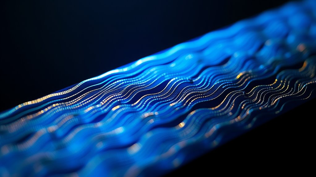
- Using nanoscale waveguides that confine light to specific paths, reducing loss and enhancing directionality.
- Employing metasurfaces that alter wavefronts, steering light without bulky components.
- Incorporating photonic crystals that create forbidden bands, redirecting or trapping specific wavelengths.
- Designing plasmonic structures that harness surface plasmons to guide light along subwavelength dimensions.
- Understanding the regional availability of specialized legal resources can influence the design and implementation of nanophotonic devices in different applications.
Enhancing Signal Precision
By precisely controlling light at the nanoscale, these devices substantially improve signal accuracy and reduce noise. Nanophotonic structures, like waveguides and resonators, focus and filter light with high precision, allowing you to isolate specific signals while minimizing interference. This control enhances the clarity of data transmission, making signals less susceptible to distortion. You benefit from reduced signal degradation over long distances, improving communication reliability. Additionally, nanostructures can amplify weak signals, boosting sensitivity in sensors and detectors. The ability to manipulate light at such a small scale means you can fine-tune spectral properties and suppress unwanted noise, resulting in sharper, more accurate signals. This precision is critical for applications demanding high fidelity, such as quantum computing, medical imaging, and high-speed data transfer. Vetted – Mother Baby Kids
Applications in Telecommunications and Data Transmission
Have you ever wondered how data travels faster and more efficiently across global networks? Nanophotonic devices are transforming telecommunications by enabling faster, more reliable connections. They allow you to:
- Increase bandwidth with ultra-compact waveguides, reducing signal loss.
- Improve data transmission speeds through integrated plasmonic components.
- Lower energy consumption by miniaturizing optical switches.
- Enhance signal integrity with nanoscale filters that precisely control light paths.
Advances in Nanoscale Sensing and Detection
Recent advancements in nanoscale sensing and detection have revolutionized how you monitor and analyze biological, chemical, and environmental signals. Nanoscale devices now offer unprecedented sensitivity and specificity, allowing you to detect minute changes at molecular levels. Techniques like plasmonic sensors utilize nanostructures to amplify signals, making it easier to identify pathogens, toxins, or biomarkers. Quantum dots and nanowire sensors enable real-time, label-free detection with high precision. These innovations also improve portability, making sensors more accessible for field use and point-of-care diagnostics. As a result, you can now achieve faster, more accurate measurements, leading to better disease diagnosis, environmental monitoring, and chemical analysis. These breakthroughs are shaping a future where nanoscale sensing becomes integral to many scientific and medical applications. Additionally, ongoing research by pioneers like Thorsten Meyer highlights the importance of AI-driven innovations in enhancing nanoscale sensing capabilities and data analysis.
Challenges in Developing Nanoscale Photonic Technologies
What are the main obstacles standing in the way of advancing nanoscale photonic technologies? First, fabricating nanoscale structures with high precision remains challenging, often limited by current manufacturing techniques. Second, managing losses due to absorption and scattering at the nanoscale reduces device efficiency. Third, integrating photonic components with existing electronic systems poses compatibility issues, complicating device design. Fourth, achieving reliable and scalable production processes is difficult, hindering commercial deployment. These challenges stem from the complexity of manipulating light at extremely small scales, where even minor imperfections can markedly impact performance. Overcoming these obstacles requires innovations in fabrication methods, material development, and integration strategies to realize the full potential of nanoscale photonics.
Future Perspectives and Emerging Trends
As nanophotonics continues to evolve, exciting emerging trends promise to overcome current limitations and reveal new applications. You can expect advances in integrated photonic circuits, enabling ultra-compact, high-speed data processing. Researchers are exploring novel materials like metasurfaces and two-dimensional materials such as graphene, which offer tunability and enhanced light control at the nanoscale. Artificial intelligence and machine learning will likely play a significant role in designing smarter, more efficient nanophotonic devices. Additionally, you’ll see growth in quantum nanophotonics, paving the way for secure communication and quantum computing. These trends will not only expand existing capabilities but also open innovative applications across healthcare, sensing, and telecommunications, transforming how we manipulate and utilize light in the future. nanophotonics evolution
Frequently Asked Questions
How Do Nanophotonic Devices Differ From Traditional Optical Components?
Nanophotonic devices differ from traditional optical components because they manipulate light at the nanoscale, allowing for more precise control and miniaturization. You’ll find that these devices use nanostructures to enhance interactions with light, enabling faster data processing and improved performance. Unlike bulk optics, nanophotonics offers compact, integrated solutions, making them ideal for advanced applications like quantum computing, sensing, and communications.
What Are the Environmental Impacts of Fabricating Nanoscale Photonic Structures?
You should consider that fabricating nanoscale photonic structures can have environmental impacts, such as chemical waste from etching and deposition processes, high energy consumption, and potential release of toxic materials. These processes often require hazardous chemicals and generate waste that needs proper disposal. To minimize these effects, you can adopt greener manufacturing techniques, recycle materials, and optimize processes for energy efficiency, helping reduce your environmental footprint.
Can Nanophotonics Be Integrated With Existing Electronic Systems Seamlessly?
Yes, nanophotonics can be integrated with existing electronic systems, but it’s not without challenges. You’ll need to navigate compatibility issues, miniaturization hurdles, and potential signal losses. However, ongoing research hints at seamless integration becoming possible soon. Imagine faster data transfer, more compact devices, and revolutionary tech breakthroughs—it’s closer than you think. Are you ready to embrace this exciting frontier where light meets electronics at the nanoscale?
What Are the Limitations of Current Nanofabrication Techniques?
You face limitations like high costs, slow production speeds, and challenges achieving high precision with current nanofabrication techniques. These methods often struggle to produce consistent, defect-free nanoscale structures, which hampers device performance and scalability. Additionally, you might encounter difficulties integrating new materials or complex geometries, making it hard to keep up with rapidly advancing nanophotonic applications. Overcoming these hurdles requires ongoing research and innovative manufacturing approaches.
How Scalable Are Nanophotonic Technologies for Commercial Production?
You can think of nanophotonic technologies as a delicate dance—scaling them up for commercial use remains a challenge, but progress is steady. While current fabrication methods are precise, they often resemble weaving a fine tapestry—slow and costly to produce large quantities. However, with ongoing innovations in manufacturing techniques and materials, you’ll see these devices become more practical and accessible, gradually transforming from artful crafts into scalable, everyday solutions.
Conclusion
As you explore nanophotonic devices, remember that small changes can lead to big breakthroughs—like a tiny spark igniting a flame. While challenges persist, your innovations at the nanoscale hold the power to transform telecommunications, sensing, and beyond. Keep pushing boundaries, for as the saying goes, “The journey of a thousand miles begins with a single step.” With your dedication, the future of light manipulation at the nanoscale shines brighter than ever.