
Nanowires and nanotubes are essential building blocks for nanoelectronics because of their exceptional electrical, optical, and mechanical properties. They are highly conductive, lightweight, flexible, and have a large surface area, making them ideal for transistors, sensors, and memory devices. Fabricated through methods like chemical vapor deposition and electrochemical techniques, their unique features are shaping future technology. Keep exploring to understand how these nanomaterials are revolutionizing industry and innovation.
Key Takeaways
- Nanowires and nanotubes offer exceptional electrical conductivity essential for nanoelectronic components.
- Their high surface-area-to-volume ratio enables highly sensitive sensors and reactive electronic interfaces.
- Fabrication techniques like CVD allow precise control over size, shape, and properties of nanostructures.
- They are used to develop ultra-fast transistors, dense memory devices, and flexible electronics.
- Challenges include scalable production, uniformity control, and integration into existing electronic systems.
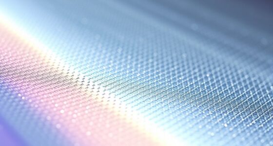
nanowire sensors
As an affiliate, we earn on qualifying purchases.
As an affiliate, we earn on qualifying purchases.
Properties and Characteristics of Nanowires and Nanotubes
Nanowires and nanotubes exhibit unique properties that set them apart from bulk materials, primarily due to their extremely small size and high aspect ratio. You’ll notice their exceptional electrical conductivity, which results from quantum confinement effects that enhance electron movement. Their high surface-area-to-volume ratio makes them highly reactive, ideal for sensing applications. Mechanically, they are incredibly strong and flexible, allowing for durable yet lightweight components. Thermal properties also differ; nanowires and nanotubes can conduct heat efficiently or insulate, depending on their composition. Additionally, their optical properties are remarkable—they can absorb and emit light at specific wavelengths, enabling advanced optoelectronic devices. These characteristics make nanowires and nanotubes versatile building blocks for cutting-edge nanoelectronics and nanotechnology innovations. Their tunable electronic and optical properties further expand their potential in nanotechnology applications such as sensors, transistors, and energy storage devices.
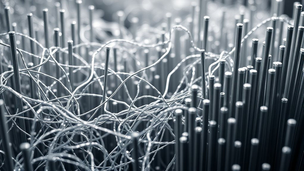
carbon nanotubes for electronics
As an affiliate, we earn on qualifying purchases.
As an affiliate, we earn on qualifying purchases.
Fabrication Techniques and Material Choices

To fabricate nanowires and nanotubes, researchers employ a variety of techniques that allow precise control over their size, shape, and material composition. Chemical vapor deposition (CVD) is common, where gases react on a heated substrate to form these nanostructures. You might also use electrochemical methods, such as anodic aluminum oxide templates, to grow uniform nanotubes. Physical techniques like laser ablation and molecular beam epitaxy provide high purity and control over crystalline quality. Material choices depend on your application’s needs; common options include silicon, carbon (graphene and carbon nanotubes), and metal oxides. Each method influences the nanostructure’s properties, enabling you to tailor electrical, optical, and mechanical characteristics essential for advanced nanoelectronic devices. Selecting the appropriate fabrication technique and material is vital for optimizing device performance.
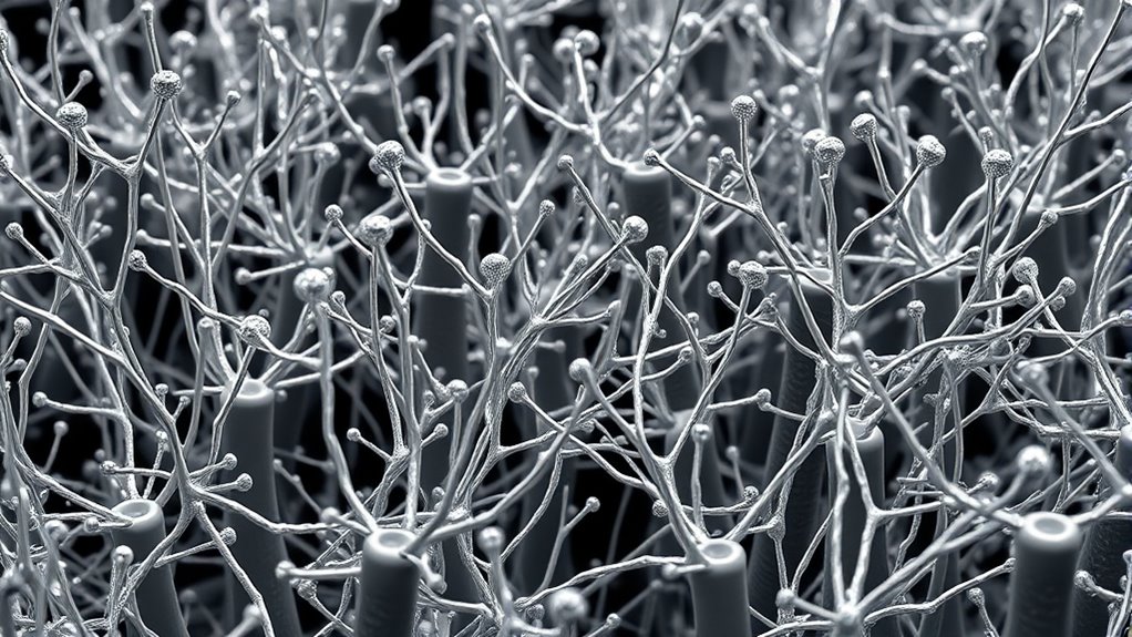
nanowire transistors
As an affiliate, we earn on qualifying purchases.
As an affiliate, we earn on qualifying purchases.
Applications in Nanoelectronic Devices

The unique electrical and mechanical properties of nanowires and nanotubes make them integral to advancing nanoelectronic devices. You can leverage their high conductivity to create ultra-fast transistors and interconnects. Their small size enables the development of highly dense memory storage, increasing capacity without bulk. You might use nanotubes as sensors, detecting chemical or biological signals with exceptional sensitivity. Additionally, their flexibility allows integration into wearable tech and flexible electronics, expanding application possibilities. These materials also serve as core components in quantum computing elements, enabling faster processing speeds. Their versatility not only improves device performance but also opens new avenues for innovation across nanoelectronics. As a result, nanowires and nanotubes are transforming how you design, build, and optimize miniaturized electronic systems. Ongoing research into AI safety and vulnerabilities continues to shape the development of secure and reliable nanoelectronic technologies.]
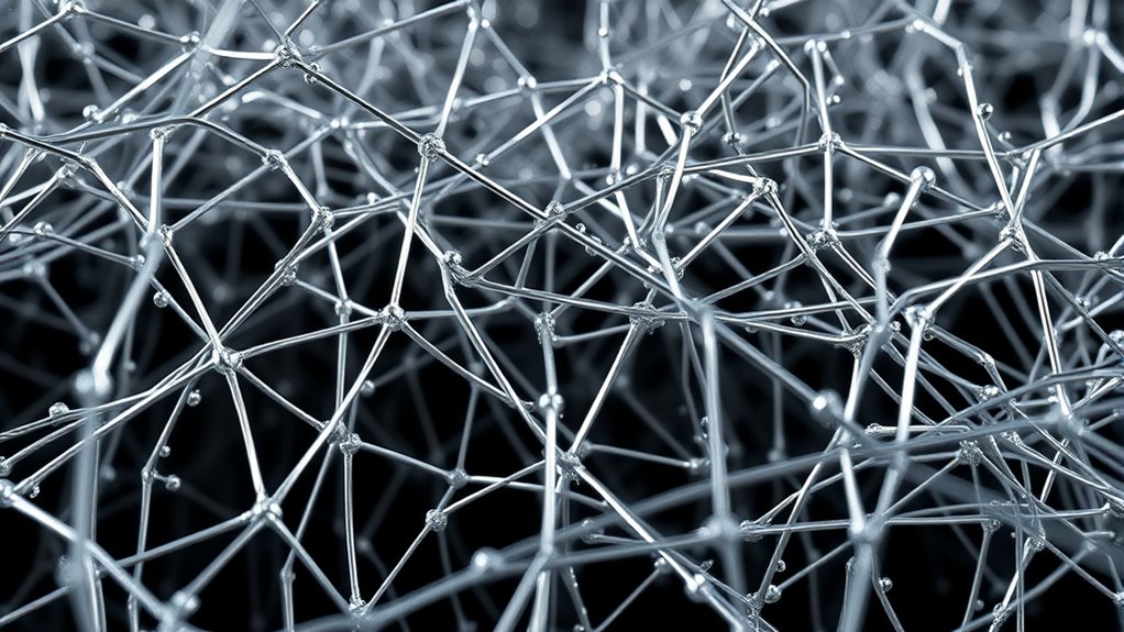
As an affiliate, we earn on qualifying purchases. As an affiliate, we earn on qualifying purchases.flexible nanoelectronics
Challenges and Future Directions
Despite their remarkable potential, nanowires and nanotubes face significant challenges that hinder widespread adoption. One major hurdle is controlling their synthesis to achieve uniform size, shape, and properties, which is vital for reliable device performance. Scalability also remains an issue; producing these nanostructures consistently on a commercial scale is difficult and costly. Additionally, integrating them into existing fabrication processes requires overcoming compatibility and stability concerns. Environmental and health impacts pose further challenges, as long-term effects of nanomaterials are not fully understood. Developing quality control measures and establishing standardized testing are crucial steps toward addressing these concerns. For future progress, research must focus on developing scalable, cost-effective production methods and improving the understanding of nanomaterial behavior. Addressing these challenges will be essential to release the full potential of nanowires and nanotubes in next-generation nanoelectronics.
Impact on Technology and Industry

Nanowires and nanotubes are transforming various industries by enabling the development of smaller, faster, and more efficient devices. You’ll see their impact in several ways:
- They improve electronics by increasing performance and reducing size in transistors and sensors.
- They enable advancements in energy storage, making batteries and supercapacitors more powerful.
- They open new possibilities in medical tech, such as highly sensitive biosensors and targeted drug delivery.
- They revolutionize materials science by creating stronger, lighter, and more flexible materials.
- Home decoration applications are emerging as these nanostructures can influence the development of innovative, durable, and aesthetically versatile materials.
These innovations lead to faster data processing, longer-lasting batteries, and smarter medical devices. As a result, industries become more competitive, and new markets emerge, pushing technology forward at an unprecedented pace.
Frequently Asked Questions
How Do Environmental Factors Affect Nanowire and Nanotube Stability?
Environmental factors like temperature, humidity, and chemical exposure substantially impact nanowire and nanotube stability. You might notice that high temperatures cause these structures to degrade or change properties, while moisture can lead to corrosion or oxidation. Chemical agents can weaken or dissolve them. To guarantee durability, you should protect nanomaterials from extreme conditions, use proper coatings, and control the environment during manufacturing and operation.
What Are the Cost Implications of Large-Scale Nanowire and Nanotube Production?
While large-scale production of nanowires and nanotubes might seem costly upfront, the investment can pay off through more efficient, smaller devices in the long run. You’ll likely see savings from optimized manufacturing processes and economies of scale. Although initial setup costs are higher, the potential for widespread application and improved performance makes the overall financial picture more promising, encouraging you to view it as a worthwhile venture.
Can Nanowires and Nanotubes Be Integrated With Existing Semiconductor Technologies?
Yes, you can integrate nanowires and nanotubes with existing semiconductor technologies. They’re compatible with current fabrication processes, allowing you to enhance device performance and miniaturize components. You’ll find that techniques like chemical vapor deposition and lithography enable precise placement and connection. This integration helps you develop faster, more efficient electronics, pushing the boundaries of innovation while leveraging established manufacturing infrastructure.
How Do Surface Defects Influence Electronic Properties at the Nanoscale?
Like a sculptor revealing hidden flaws, surface defects at the nanoscale profoundly influence electronic properties. You’ll find that these imperfections can trap charge carriers, reduce conductivity, or create localized states, much like ripples disturbing a calm pond. They often act as scattering centers, hindering electron flow, or induce unwanted energy states. Managing these defects is essential, as they directly affect device performance, reliability, and the potential for miniaturization in nanoelectronics.
What Are the Long-Term Reliability Concerns for Nanoelectronic Components?
You should be aware that long-term reliability concerns for nanoelectronic components include material degradation, such as electromigration, and the impact of surface defects. These issues can cause device failure over time due to increased resistance or structural breakdown. You need to contemplate environmental factors like humidity and temperature fluctuations, which may accelerate degradation. Regular testing and protective coatings can help mitigate these risks and extend the lifespan of your nanoelectronic devices.
Conclusion
You now see how nanowires and nanotubes are the building blocks shaping the future of nanoelectronics. Like tiny bridges connecting innovation to reality, their unique properties reveal new possibilities in device performance and miniaturization. While challenges remain, your understanding of these nanostructures positions you at the forefront of technological evolution. Embrace this frontier, because in the world of nanoelectronics, you’re holding the key to transforming the tiniest components into giants of progress.