
Organic nanomaterials, especially conducting polymers and organic semiconductors, enable flexible, lightweight, and eco-friendly electronic devices. These materials offer high conductivity, tunable properties, and versatile processing methods like solution coating and layer assembly. They power applications in wearable tech, displays, and solar cells. While challenges remain around scalability and stability, ongoing advances improve performance and sustainability. Continue exploring to discover how these innovative materials are shaping the future of electronics.
Key Takeaways
- Conducting polymers are key organic nanomaterials enabling electrical conductivity in flexible electronic devices.
- Organic semiconductors facilitate efficient charge transport for applications like OLEDs, solar cells, and sensors.
- Synthesis methods include chemical, electrochemical, and controlled polymerization techniques such as RAFT.
- Fabrication strategies like layer-by-layer assembly and solution processing enable scalable device manufacturing.
- Advantages include flexibility, lightweight design, biodegradability, and cost-effectiveness over inorganic materials.

3D Printed Conducting Polymers (Smart 3D/4D Printing)
As an affiliate, we earn on qualifying purchases.
As an affiliate, we earn on qualifying purchases.
Overview of Organic Nanomaterials

Have you ever wondered what makes organic nanomaterials unique? These tiny materials are distinguished by their biodegradability and biocompatibility, making them highly suitable for medical and environmental applications. Unlike inorganic counterparts, organic nanomaterials naturally break down in the body or environment, reducing long-term pollution. Their biocompatibility ensures they can interact safely with biological systems without causing adverse reactions. This dual advantage allows you to develop eco-friendly medical devices, drug delivery systems, and biodegradable sensors. Organic nanomaterials are composed of carbon-based molecules, which provide flexibility in design and functionalization. Their ability to seamlessly integrate into biological environments makes them a promising foundation for innovative solutions that are both effective and sustainable. Additionally, easy to clean and maintain features can prolong the lifespan of devices made from organic nanomaterials, further supporting their sustainable use.

Rugged Sturdy Solar Cell Experiment Kit, Energy Power Generation Equipment for Junior High School, Easy, Drive Motor with Solar Battery, Convert Solar Energy into Electr
Easy : Simple to set up and use, making it ideal for junior high school students to learn…
As an affiliate, we earn on qualifying purchases.
As an affiliate, we earn on qualifying purchases.
Properties of Conducting Polymers

Conducting polymers can vary widely in electrical conductivity, allowing you to tailor them for specific applications. They also offer impressive mechanical flexibility, making them suitable for flexible electronics. Understanding these properties helps you optimize their performance in your projects. Additionally, advancements in projector technology continue to expand their potential uses in display and imaging systems.
Electrical Conductivity Variability
Electrical conductivity in conducting polymers can vary considerably depending on their molecular structure and processing conditions. Doping effects play a pivotal role, as introducing dopants can markedly enhance conductivity by increasing charge carrier density. Variability arises because different doping levels, types, and methods alter the polymer’s electronic properties, leading to fluctuations in conductivity. Factors such as polymer chain alignment, crystallinity, and defect presence also contribute to this variability. Processing parameters like temperature, solvent choice, and film formation techniques impact how uniformly dopants distribute, further affecting electrical performance. This inherent electrical conductivity variability means that achieving consistent, reliable results requires precise control over doping and processing conditions. Understanding these influences helps optimize conducting polymers for electronic applications where predictable electrical behavior is essential.
Mechanical Flexibility Traits
The molecular structure and processing methods that influence electrical conductivity also considerably affect the mechanical flexibility of conducting polymers. Their flexibility depends on chain alignment, molecular weight, and cross-linking, which determine how well they bend without breaking. You should consider biocompatibility considerations, especially when using these materials in flexible, implantable devices, as mechanical stress can impact stability and performance. Thermal expansion plays a role too; polymers with low thermal expansion coefficients maintain flexibility across temperature changes, reducing cracking or delamination. Proper processing techniques, like doping and film casting, enhance flexibility by controlling the polymer’s morphology. Overall, understanding these traits helps optimize conducting polymers for flexible electronics, ensuring durability and comfort in real-world applications.
Wearable biosensor with organic nanomaterials
As an affiliate, we earn on qualifying purchases.
As an affiliate, we earn on qualifying purchases.
Types of Organic Semiconductors

Organic semiconductors come in several distinct types, each with unique properties suited for different applications. You’ll find small-molecule semiconductors, which offer high purity and precise control over structures, ideal for OLEDs and solar cells. Conjugated polymers, another key type, provide excellent flexibility and processability, making them perfect for wearable electronics. Additionally, hybrid organic materials combine organic semiconductors with inorganic components, enhancing performance and stability. These hybrid systems leverage the advantages of both worlds, such as improved charge transport and mechanical flexibility. Understanding the different organic semiconductor types helps you select the best material for your specific device needs. By exploring these options, you can optimize performance in applications like flexible displays, sensors, and energy harvesting devices. Advances in material design continue to expand the potential uses of organic semiconductors in various cutting-edge technologies.

Introduction to Organic Electronic Devices
As an affiliate, we earn on qualifying purchases.
As an affiliate, we earn on qualifying purchases.
Synthesis and Fabrication Techniques

You can create organic nanomaterials using various polymerization methods that control molecular structure. Layer-by-layer assembly allows precise building of thin, functional coatings, while solution processing offers scalable fabrication options. Understanding these techniques helps you tailor nanomaterials for specific applications effectively. Additionally, mastering fabrication techniques is essential for optimizing the performance and stability of organic semiconductors.
Polymerization Methods Employed
Polymerization methods for organic nanomaterials encompass a variety of synthesis and fabrication techniques tailored to produce nanoscale polymers with specific properties. Your choice of polymerization technique directly influences nanostructure control and material performance. Here are three common methods:
- Chemical polymerization: You initiate reactions with chemical oxidants or catalysts, allowing precise control over polymer chain length and morphology.
- Electrochemical polymerization: Applying an electric current, you can deposit conducting polymers directly onto electrodes, enabling nanoscale patterning.
- Reversible addition-fragmentation chain transfer (RAFT): This controlled radical polymerization technique offers fine-tuned molecular weights and architectures, essential for nanoscale applications.
Layer-by-Layer Assembly Techniques
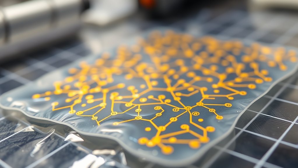
Layer-by-layer (LbL) assembly is a versatile technique for fabricating nanostructured materials by sequentially depositing alternating layers of complementary materials. This method allows you to control nanomaterial layering with remarkable assembly precision. You can tailor properties like conductivity, permeability, and surface functionality by adjusting layer composition and thickness. The process involves immersion, rinsing, and drying steps, enabling precise control at each stage. LbL assembly is ideal for creating thin films, sensors, and nanocomposites. Its simplicity and scalability make it attractive for organic nanomaterials. To illustrate, consider the table below, which highlights key features and applications of LbL assembly:
| Feature | Application |
|---|---|
| Layer control | Organic electronics |
| Precise nanomaterial layering | Sensors and membranes |
| Versatility in materials | Flexible device fabrication |
| Surface functionalization | Biointerfaces |
| Scalability | Commercial production |
Solution Processing Strategies
How can solution processing strategies revolutionize the fabrication of organic nanomaterials? They enable simple, scalable, and cost-effective methods to create high-quality devices. By carefully considering solvent selection, you can optimize the solubility and film formation of conducting polymers and organic semiconductors. Deposition techniques such as spin coating, doctor blading, and inkjet printing allow precise control over film thickness and uniformity. Here’s how these strategies make a difference:
- Solvent selection influences the morphology and electrical properties of the resulting nanomaterials.
- Advanced deposition techniques improve layer quality and scalability for commercial applications.
- Combining these methods offers versatile pathways to tailor device performance and streamline manufacturing processes.
Applications in Flexible Electronics
Organic nanomaterials are revolutionizing flexible electronics by enabling the development of lightweight, bendable, and durable devices. Their inherent flexibility and conductivity make them ideal for wearable sensors, foldable displays, and flexible solar cells. However, biodegradability concerns arise with increasing adoption, prompting you to explore environmentally friendly disposal methods and sustainable materials. To make these technologies more accessible, cost reduction strategies are crucial, such as scalable synthesis techniques and material optimization to lower production costs. Additionally, incorporating innovations in CAD design can enhance device performance and manufacturing efficiency. By addressing biodegradability concerns and adopting cost-effective approaches, you can accelerate the integration of organic nanomaterials into commercial flexible electronic devices. This progress ensures that flexible electronics not only perform well but also align with environmental sustainability and economic viability.
Advantages Over Inorganic Materials

Organic nanomaterials offer distinct advantages over inorganic materials, primarily due to their inherent flexibility and lightweight nature. These features translate into significant benefits, including:
- Cost reduction: Organic materials are generally less expensive to produce and process, making them more accessible for large-scale applications.
- Enhanced biocompatibility: Their compatibility with biological systems opens doors for medical devices and implants without adverse reactions.
- Ease of fabrication: Organic nanomaterials can be processed using simple, low-temperature methods, saving time and energy compared to inorganic counterparts.
- AI safety measures are crucial to ensure these materials are developed and deployed responsibly, minimizing potential risks.
These advantages make organic nanomaterials a compelling choice for innovative technologies, especially where flexibility, affordability, and biological compatibility are vital.
Challenges and Limitations

Despite their numerous advantages, organic nanomaterials face significant challenges that hinder widespread adoption. Scalability issues make it difficult to produce these materials consistently and cost-effectively on a large scale, limiting their commercial use. You might find that manufacturing processes are complex, requiring precise control over synthesis conditions, which can be costly and time-consuming. Additionally, toxicity concerns raise questions about environmental impact and safety during production, handling, and disposal. Organic nanomaterials may release harmful byproducts or pose risks to human health, creating regulatory hurdles. These limitations mean you need to carefully consider both production feasibility and safety issues before integrating organic nanomaterials into practical applications. Addressing these challenges is essential to ethical hacking their full potential in various technological fields.
Recent Advances in Material Performance

Recent advances have markedly boosted the performance of organic nanomaterials, making them more efficient for various applications. You’ll notice improved charge mobility, which enhances electronic device speed and efficiency. Additionally, researchers have achieved better stability and durability, extending the lifespan and reliability of these materials.
Enhanced Charge Mobility
How have recent innovations enhanced charge mobility in nanomaterials? They’ve markedly improved charge transport and conductivity enhancement, making organic nanomaterials more efficient. Here are key advances:
- Molecular Design: Tailoring molecular structures reduces trap states, boosting charge mobility.
- Doping Techniques: Introducing dopants increases carrier concentration, enhancing conductivity.
- Alignment Strategies: Using methods like solution processing aligns polymer chains, facilitating smoother charge flow.
These innovations enable better charge transport pathways, resulting in higher mobility. As a result, organic semiconductors now demonstrate improved performance in electronic devices. By focusing on molecular architecture, doping, and alignment, researchers have discovered new levels of efficiency. Your understanding of these advances highlights how material engineering directly impacts charge transport and conductivity enhancement, pushing organic nanomaterials toward broader applications.
Improved Stability and Durability
Advances in material engineering have considerably enhanced the stability and durability of organic nanomaterials, making them more reliable for long-term applications. Through stability enhancement techniques, you can now markedly slow nanomaterial degradation, extending device lifespan. These innovations include protective coatings, cross-linking, and improved synthesis methods that resist environmental stressors. The progress means your devices will perform consistently over time, reducing failures and maintenance costs. To evoke emotion, consider this outlook:
| Challenges Faced | Breakthroughs Achieved |
|---|---|
| Nanomaterial degradation | Enhanced stability techniques |
| Environmental damage | Longer-lasting performance |
| Reliability issues | Greater confidence in applications |
Environmental Impact and Sustainability

Organic nanomaterials are often praised for their potential to reduce environmental impact, but it’s important to contemplate their sustainability throughout their life cycle. You should consider factors like recycling challenges and the ecological footprint. Here are key points to keep in mind:
- Recycling challenges can hinder the reuse of organic nanomaterials, complicating waste management.
- Their production often involves energy-intensive processes, increasing the ecological footprint.
- Sustainable sourcing and greener synthesis methods can help minimize environmental impact.
- Incorporating sustainable practices in the development and deployment of organic nanomaterials is essential for truly reducing their environmental footprint.
Future Perspectives and Emerging Trends

As research into organic nanomaterials progresses, emerging trends are shaping a more sustainable and versatile future for this field. You’ll see a growing focus on developing smart wearable devices that leverage organic conductors and semiconductors for improved flexibility and durability. These materials enable seamless integration into clothing and accessories, enhancing user comfort and functionality. Additionally, energy harvesting becomes a key trend, with organic nanomaterials powering self-sufficient systems that convert ambient energy into usable electrical power. This approach reduces reliance on batteries and promotes eco-friendly solutions. You can expect innovations that combine these trends, creating smarter, more sustainable technologies. By embracing these developments, you’ll contribute to advancing organic nanomaterials toward practical, real-world applications that benefit both users and the environment. Furthermore, fostering a creative mindset can accelerate innovation in this field, as embracing failure as a learning opportunity encourages researchers to experiment and discover novel solutions.
Frequently Asked Questions
How Do Organic Nanomaterials Compare to Biological Systems?
You’ll find that organic nanomaterials often mimic biological systems through their structural complexity, allowing for sophisticated functions. Their biocompatibility advantages make them suitable for medical applications, unlike many inorganic materials. Organic nanomaterials can interact more seamlessly with biological tissues, offering better integration and reduced rejection. This similarity in structure and compatibility means they can be tailored for bioelectronics, sensors, and drug delivery, bridging the gap between synthetic materials and living systems.
What Are the Cost Implications of Large-Scale Production?
Like a rising tide, large-scale production impacts your costs through a complex interplay of factors. You’ll find that thorough cost analysis reveals economies of scale, lowering per-unit expenses. However, manufacturing scalability can introduce challenges, such as equipment investment and process optimization. These factors shape your overall budget, making it essential to guarantee your initial costs with long-term savings. Embracing this rhythm ensures your production remains efficient and financially sustainable.
How Do Organic Semiconductors Perform in Extreme Environmental Conditions?
You’ll find that organic semiconductors generally struggle with extreme environmental conditions, especially concerning temperature stability and moisture resistance. High temperatures can cause degradation, reducing performance and lifespan, while moisture can lead to corrosion and electrical failures. To improve their durability, researchers are working on encapsulation techniques and material modifications, but currently, these materials perform best within moderate conditions and need protection in harsher environments.
Can Organic Nanomaterials Be Recycled or Reused Effectively?
You can recycle or reuse organic nanomaterials, but recycling challenges exist due to their complex structures and small sizes. Effective reuse potential depends on developing sustainable methods that separate and recover active components without degrading performance. Advances in green chemistry and innovative recycling techniques are making it easier to repurpose these materials, reducing waste and extending their lifespan. With continued research, organic nanomaterials can become more environmentally friendly and easier to recycle effectively.
What Are the Safety Considerations for Manufacturing and Disposal?
You should consider toxicity risks during manufacturing and disposal of organic nanomaterials, as some may release harmful chemicals or nanoparticles. Guarantee proper waste management by following safety protocols to prevent environmental contamination and health hazards. Use protective equipment, proper ventilation, and disposal methods designed for nanomaterials. Regularly monitor emissions and waste to minimize potential risks, and stay updated on safety regulations to protect yourself and the environment effectively.
Conclusion
As you explore organic nanomaterials, it’s fascinating to see how conducting polymers and semiconductors intertwine like threads in a vibrant fabric. Their promising applications in flexible electronics feel almost within reach, yet challenges remind you that innovation is a continuous journey. With recent breakthroughs and a focus on sustainability, you’re witnessing a future where these materials could seamlessly integrate into your everyday life, transforming technology in ways you might not yet imagine.