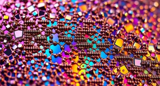
Photonic crystals in nano devices are engineered structures that manipulate light by controlling their periodic dielectric properties. They create forbidden frequency ranges called bandgaps and localized defect modes that trap or guide light precisely. This allows you to develop compact, efficient optical components like waveguides, lasers, and sensors with minimal loss. If you explore further, you’ll discover how these innovations lead to advanced applications in communication, sensing, and computing.
Key Takeaways
- Photonic crystals manipulate electromagnetic waves at the nanoscale through engineered periodic dielectric structures.
- Bandgap engineering in photonic crystals enables selective filtering and miniaturization of optical components.
- Introducing defects creates localized modes, serving as optical cavities for enhanced sensing and laser performance.
- Combining bandgap and defect modes allows customizable light control for efficient resonators and filters.
- They enable the development of compact, energy-efficient nano devices for advanced optical communication, sensing, and computing.
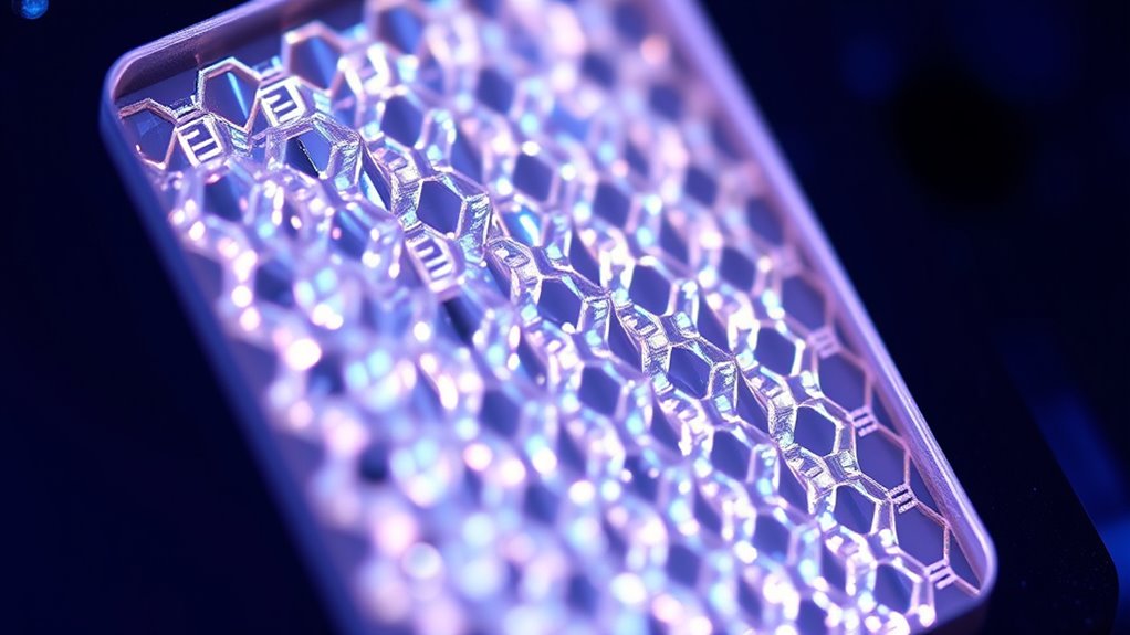
Have you ever wondered how light can be precisely controlled at the nanoscale? That’s where photonic crystals in nano devices come into play. These structures are engineered materials with periodic dielectric variations, designed to manipulate and control electromagnetic waves with remarkable accuracy. When you incorporate photonic crystals into nano devices, you harness their unique ability to affect light propagation in ways that traditional materials can’t achieve. This control opens doors to innovations in optical communications, sensing, and computing.
One of the key aspects of photonic crystals is their capacity for bandgap engineering. Think of it like creating a custom filter that blocks certain light frequencies while allowing others to pass. By adjusting the periodicity and dielectric contrast within the crystal, you can tailor the photonic bandgap—the range of forbidden light frequencies—precisely to your needs. This ability to engineer the bandgap is essential for developing highly efficient waveguides, lasers, and filters at the nanoscale. It allows you to confine and direct light with minimal losses, making devices more compact and energy-efficient.
In addition to bandgap engineering, defect modes play a critical role in the function of photonic crystal-based nano devices. When you introduce intentional defects into the periodic structure, you create localized states within the bandgap. These defect modes act like optical cavities, trapping light at specific frequencies. This is incredibly useful for designing highly sensitive sensors, where even minute changes in the environment can shift the defect mode’s resonance. It’s also essential for creating narrow-linewidth lasers and filters, where controlling the light’s behavior at the defect site enhances performance enormously. Recognizing the importance of material properties is vital for optimizing device performance at the nanoscale.
By combining these two concepts—bandgap engineering and defect modes—you can develop nano devices with highly customizable optical properties. For instance, you can design a photonic crystal resonator that captures and releases light at precise wavelengths, boosting the device’s efficiency. Or, you could create a sensor that detects chemical or biological agents by observing shifts in defect modes caused by environmental changes. The versatility of photonic crystals at the nanoscale means you’re not just controlling light—you’re tailoring its interaction with matter to suit a wide array of cutting-edge applications.
Ultimately, understanding and utilizing the principles of photonic crystals in nano devices give you a powerful toolkit. You can manipulate light with unprecedented precision, making possible the next generation of optical technologies. Whether for communication, sensing, or computing, these structures enable innovations that were once thought impossible, all by carefully designing their bandgaps and defect modes.
Frequently Asked Questions
How Do Photonic Crystals Influence Quantum Dot Performance?
Photonic crystals enhance quantum dot performance by providing optical confinement, which increases light-matter interaction. They allow you to control emission properties, directing photons efficiently and reducing losses. This leads to brighter, more stable quantum dots with tailored emission wavelengths. By manipulating the photonic environment, you can optimize device functionalities, improving applications like quantum computing and advanced photonics. Overall, photonic crystals enable you to precisely control and boost quantum dot performance.
What Are the Manufacturing Challenges for Integrating Photonic Crystals?
You face significant manufacturing challenges when integrating photonic crystals, as precision in fabrication is vital yet difficult to achieve. Material compatibility complicates the process further, requiring careful selection to prevent defects or damage. While advanced lithography offers high resolution, aligning intricate structures at the nanoscale remains demanding. Balancing these factors is essential, as even minor imperfections can impede performance and scalability, highlighting the delicate dance between innovation and technical limitation.
Can Photonic Crystals Be Used in Flexible Nano Devices?
Yes, you can use photonic crystals in flexible nano devices. You’ll need to focus on flexible substrates like polymers to guarantee mechanical integration, allowing the crystals to bend and stretch without losing their optical properties. By carefully designing the structure and choosing suitable materials, you can develop flexible photonic devices that maintain functionality under mechanical stress, opening new possibilities for wearable tech, flexible displays, and adaptive optical systems.
How Do Temperature Variations Affect Photonic Crystal Behavior?
Temperature variations can notably impact photonic crystal behavior through thermal effects, altering their optical properties. For example, if you imagine a sensor embedded with photonic crystals, rising temperatures might cause a shift in the crystal’s bandgap, reducing temperature stability. This means that maintaining consistent performance requires managing thermal effects carefully, perhaps through material selection or cooling techniques, to ensure the device remains reliable across different temperature ranges.
Are There Environmental Impacts Associated With Photonic Crystal Production?
Yes, there are environmental concerns linked to photonic crystal production. You might face sustainability challenges due to the use of rare materials and energy-intensive manufacturing processes. These practices can contribute to resource depletion and pollution. To minimize impact, consider adopting greener methods, recycling materials, and improving energy efficiency. Addressing these sustainability challenges helps reduce environmental footprints and promotes responsible development of photonic crystal technologies.
Conclusion
Think of photonic crystals as the guiding stars in your nano device universe, illuminating paths you once thought impossible. They act as the heartbeat, syncing light with precision, turning complex ideas into elegant solutions. As you harness their power, remember you’re holding a tiny lighthouse, guiding photons safely through the darkest depths. Embrace this symbolism, and you’ll see how these crystals transform your innovations into shining beacons of progress, lighting the way for future breakthroughs.