
Atomic Force Microscopy (AFM) helps you analyze nanomachines at atomic resolution by using a sharp tip to scan surfaces and measure forces. It offers detailed imaging, mechanical property data, and surface interaction insights. You can also manipulate and fabricate nanoscale components with AFM. Recent advances improve sensitivity and resolution, expanding capabilities across engineering and biomedical applications. Exploring this technology further reveals how AFM can unveil deeper understanding of nanomachine behavior and design.
Key Takeaways
- AFM provides high-resolution imaging of nanomachine surface structures at near-atomic detail.
- It enables measurement of mechanical properties like stiffness and elasticity of nanomachines.
- Tip functionalization allows targeted interaction analysis of specific molecules within nanodevices.
- Dynamic modes and advanced techniques improve resolution, reduce damage, and reveal electronic interactions.
- Thermal imaging and force spectroscopy facilitate understanding of thermal behavior and surface interactions in nanomachines.
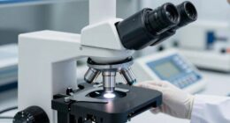
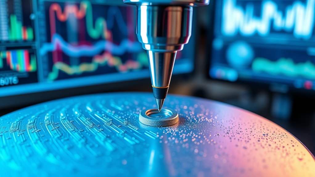
Atomic Force Microscope AFM
As an affiliate, we earn on qualifying purchases.
As an affiliate, we earn on qualifying purchases.
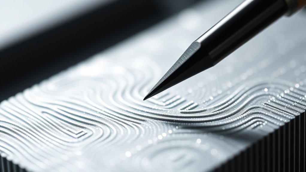
Principles and Techniques of AFM in Nanomachine Analysis
Atomic Force Microscopy (AFM) operates by scanning a sharp tip across a sample surface to measure minute forces between the tip and the surface atoms. To guarantee accurate force measurement, force calibration is essential; it helps you relate deflections to actual force values, increasing reliability. Tip functionalization enhances AFM‘s versatility by attaching specific molecules or coatings to the tip, enabling you to target particular surface features or interactions. Proper calibration and functionalization are critical for precise nanomachine analysis, as they influence the sensitivity and specificity of your measurements. Additionally, understanding the contrast ratio helps you interpret the quality of the images obtained, ensuring accurate characterization of nanostructures. By carefully calibrating your AFM setup and customizing your tip, you can obtain detailed, reliable data on nanostructures, paving the way for insightful analysis of nanomachine properties and behaviors at the atomic level.
AFM tip functionalization kit
As an affiliate, we earn on qualifying purchases.
As an affiliate, we earn on qualifying purchases.
Visualizing Nanostructures With High Resolution
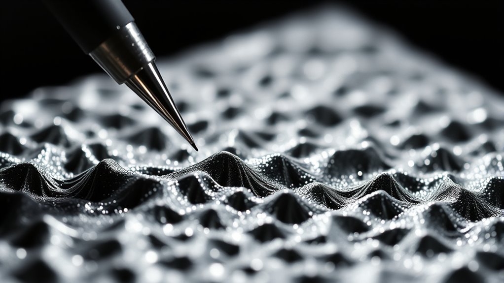
High-resolution visualization of nanostructures is essential for understanding their detailed architecture and functional properties. With atomic force microscopy, you can achieve molecular imaging that reveals surface features at near-atomic precision. This capability allows you to analyze surface roughness, providing insights into how nanomachines interact with their environment. To optimize your imaging efforts, consider these key points:
Achieve near-atomic imaging of nanostructures with AFM by optimizing tips and scanning parameters.
- Use sharp, well-calibrated tips for clearer, detailed images.
- Adjust scanning parameters to balance resolution and surface stability.
- Analyze surface roughness data to identify variations that influence nanomachine performance. Continuously improving your technique helps ensure high-quality, reliable results.
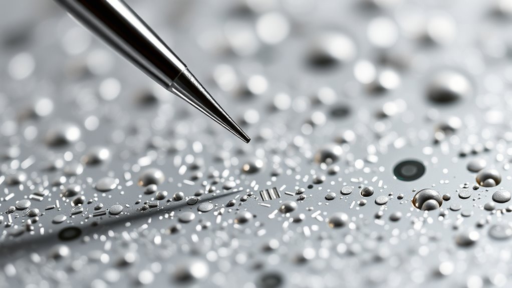
nanoscale force measurement instrument
As an affiliate, we earn on qualifying purchases.
As an affiliate, we earn on qualifying purchases.
Mechanical Property Measurements at the Nanoscale
Measuring mechanical properties at the nanoscale provides critical insights into how materials and nanostructures behave under stress. Using AFM, you can determine properties like stiffness, elasticity, and hardness with high precision. These measurements are essential for biocompatibility testing, ensuring nanomaterials won’t cause adverse reactions in biological environments. They also help assess thermal conductivity, revealing how heat transfers through nanostructures, which impacts device performance. By applying force curves and indentation techniques, you can evaluate how nanomaterials deform and recover, providing data indispensable for designing robust nanomachines. This approach enables you to link mechanical behavior directly to material composition and structure, ensuring your nanodevices meet both functional and safety standards at the microscopic level. Additionally, understanding and mitigating AI vulnerabilities in the design process can improve the reliability and safety of nanotechnologies.
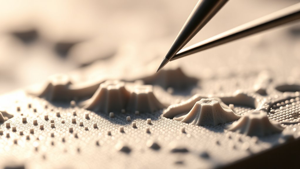
high-resolution atomic force microscope
As an affiliate, we earn on qualifying purchases.
As an affiliate, we earn on qualifying purchases.
Surface Interactions and Adhesion Studies
Understanding tip-sample forces is essential for analyzing surface interactions at the nanoscale. You can use various adhesion measurement techniques to quantify how surfaces stick and interact. These methods provide critical insights into material properties and surface chemistry.
Tip-Sample Forces
Tip-sample forces are fundamental to the operation of atomic force microscopy, as they directly influence the interaction between the cantilever tip and the surface being studied. These forces include van der Waals, electrostatic, and capillary interactions, which you can analyze through force spectroscopy. To guarantee accurate measurements, proper tip calibration is essential. It helps you determine the cantilever’s sensitivity and spring constant, allowing precise force quantification.
Consider these key points:
- Force spectroscopy maps the force-distance relationship, revealing surface properties.
- Tip calibration ensures your force measurements are reliable.
- Understanding tip-sample forces enables you to interpret adhesion and interaction details at the nanoscale.
Adhesion Measurement Techniques
How do researchers quantify the strength of surface interactions at the nanoscale? They use adhesion measurement techniques with atomic force microscopy to directly assess forces between surfaces. These methods enable you to study biological interactions, such as cell adhesion, by measuring the forces involved in these processes. Environmental effects, like humidity or temperature, influence adhesion, so you can control conditions to understand their impact. By attaching a sample or functionalized tip to the cantilever, you can perform force-distance curves that reveal adhesion forces and energy. These measurements help you evaluate how surface properties affect nanoscale interactions, providing insights into material design, biomolecular interactions, and environmental stability. This approach is essential for understanding the complex interplay of forces governing adhesion at the nanoscale.
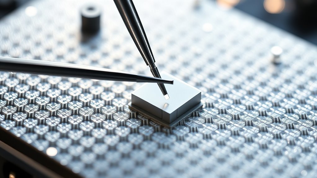
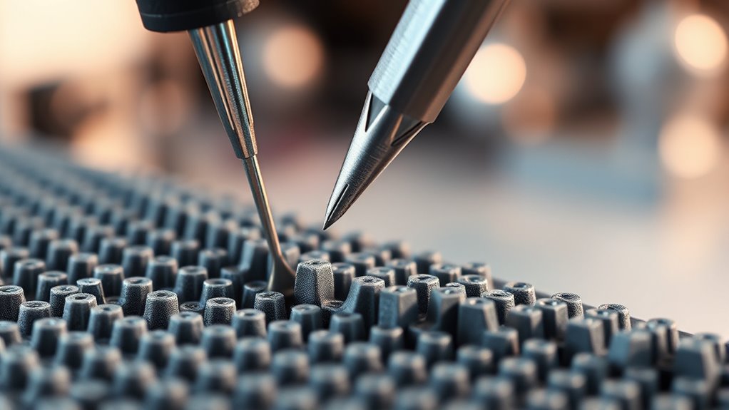
Manipulation and Fabrication of Nanomachine Components
You can use atomic force microscopy to precisely manipulate nanomachine components, allowing for exact placement and adjustment at the atomic level. By applying specialized techniques, you gain control over nanoscale features essential for device functionality. Additionally, implementing effective fabrication strategies helps you build complex nanostructures with high accuracy and reproducibility.
Precise Manipulation Techniques
Precise manipulation techniques in atomic force microscopy enable the direct assembly and modification of nanomachine components with exceptional accuracy. You leverage atomic precision to position tiny parts, ensuring exact alignment at the nanoscale. Force modulation allows you to control the interaction forces, making delicate adjustments without damaging components. Here are key techniques:
- Fine-tuning force feedback to manipulate individual atoms or molecules precisely.
- Applying atomic precision to assemble complex nanostructures layer-by-layer.
- Using force modulation to gently detach or relocate nanomachine parts without compromising integrity.
These methods give you unmatched control, facilitating the creation of functional nanodevices. By mastering atomic precision and force modulation, you can manipulate components with nanometer accuracy, opening new avenues for nanomachine development and innovation.
Nanoscale Fabrication Strategies
Nanoscale fabrication strategies harness atomic force microscopy to build and modify nanomachine components with unparalleled precision. You can perform nanoparticle assembly by positioning individual particles exactly where needed, enabling custom nanostructures. Surface patterning allows you to create intricate designs on surfaces, guiding molecular interactions or device functionalities. These techniques facilitate the precise manipulation of materials at the atomic level, essential for advanced nanomachine fabrication.
| Technique | Application | Key Benefit |
|---|---|---|
| Nanoparticle assembly | Constructing nanostructures | High precision placement |
| Surface patterning | Creating functional surfaces | Customized surface features |
| Material modification | Tailoring nanomachine properties | Enhanced device performance |
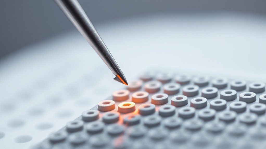
Recent Advances in AFM Methodologies for Nanotechnology
Recent advances in atomic force microscopy (AFM) methodologies have considerably expanded its capabilities for nanotechnology research. You now can explore quantum tunneling effects at the nanoscale, providing insights into electronic properties with unprecedented detail. Improvements in thermal imaging enable you to visualize temperature distributions on surfaces, which is essential for nanoelectronics and material science. Additionally, new techniques enhance sensitivity and resolution, allowing you to detect subtle surface features. Here are some key developments: 1. Integration of quantum tunneling measurements to study electronic interactions. 2. Enhanced thermal imaging for real-time temperature mapping at the nanoscale. 3. Adoption of dynamic modes that improve resolution and reduce sample damage. This progress in AFM technology further broadens the scope of nanomachine characterization, empowering you to push the boundaries of nanomachine characterization with greater precision.
Applications of AFM in Engineering and Biomedical Fields
Atomic force microscopy has become an invaluable tool in engineering and biomedical fields, enabling you to analyze surfaces and structures at the molecular and cellular levels. In biomedical diagnostics, AFM helps identify disease markers and assess cell mechanics by measuring material deformation with high precision. It allows you to visualize cellular interactions, detect early tissue changes, and study biomolecular interactions, advancing personalized medicine. In engineering, AFM is essential for evaluating material deformation under stress, helping you develop stronger, more reliable nanomaterials and coatings. Its ability to provide nanoscale topography and mechanical data makes it indispensable for quality control, failure analysis, and device optimization. Overall, AFM’s versatility enhances your capacity to innovate across both biomedical and engineering applications, pushing the frontiers of nanotechnology.
Frequently Asked Questions
How Does AFM Compare to Other Nanoscale Imaging Techniques?
You’ll find AFM offers superior resolution compared to optical microscopy, approaching atomic levels, unlike electron microscopy which provides even higher detail but requires extensive sample prep. AFM’s advantage lies in minimal sample preparation and its ability to operate in various environments, including liquids. While techniques like SEM need conductive coatings, AFM’s gentle contact preserves delicate nanomachines, making it ideal for real-world nanomachine characterization and direct surface interaction studies.
What Are Common Limitations of AFM in Nanomachine Analysis?
You might worry AFM’s resolution limitations or sample prep issues hinder your analysis, but these are manageable. AFM can struggle with soft or complex samples, leading to deformation or artifacts. Precise sample preparation is essential, yet it can be time-consuming. Despite this, AFM provides valuable surface details at the nanoscale. Knowing these limitations helps you optimize your process for clearer, more accurate nanomachine characterization.
Can AFM Be Used for Real-Time Monitoring of Nanomachine Behavior?
Yes, you can use AFM for real-time monitoring of nanomachine behavior. It provides real-time feedback and dynamic imaging, allowing you to observe nanomachines in action. Although it offers valuable insights into their movement and interactions, keep in mind that achieving high-speed imaging can be challenging due to limitations in scan speed and resolution. Still, AFM remains a powerful tool for studying nanomachine dynamics in situ.
How Does Environmental Control Affect AFM Measurements?
Environmental control markedly impacts AFM measurements by ensuring environmental stability, which reduces noise and external influences. When you maintain consistent temperature, humidity, and vibration levels, you improve measurement reproducibility. This stability helps you obtain accurate, reliable data on nanomachines, as fluctuations can distort results. By controlling these factors, you enhance the precision of your AFM measurements, making your nanomachine characterization more consistent and trustworthy over repeated experiments.
What Future Developments Are Expected in AFM Technology?
You can expect AFM technology to evolve with automated imaging becoming more sophisticated, allowing you to quickly analyze complex nanostructures. Enhanced resolution will enable you to observe even finer details at the atomic level, improving your understanding of nanomachines. Future developments will likely focus on integrating AI for better data analysis and real-time feedback, making AFM more user-friendly and precise for your nanotechnology research.
Conclusion
You now hold the key to revealing nanomachines’ secrets with AFM’s precision brush. As your microscope dances across atomic landscapes, you’ll unveil hidden structures, measure delicate forces, and craft at the tiniest scales—like a master sculptor shaping the future. With each advance, AFM transforms your vision into reality, turning nano-visions into tangible innovations. Embrace this tool, and let it be the compass guiding you through the intricate universe of nanotechnology’s endless possibilities.