The smallest machines ever built are nanoscale devices under 200 nanometers, with the Guinness World Record held by a 120-nanometer magnetoelectric nanorobot that can change shape, move, and interact with cells for potential medical applications. Advances include microrobots, ultracompact nanolasers, nanosensors, and logic devices, all pushing the limits of miniaturization. If you want to explore how these tiny machines are revolutionizing technology, keep going to uncover more.
Key Takeaways
- The smallest medical nanorobot is a 120-nanometer magnetoelectric device capable of shape-changing and remote control inside cells.
- Advances have led to nanorobots as small as 120 nm, enabling complex tasks like drug delivery and cellular interaction.
- Nanoscale photonic devices, including nanolasers and nanopixels under 50 nm, support ultradense, integrated optical systems.
- Fabrication techniques such as advanced lithography and self-assembly enable precise creation of sub-50 nm electronic and magnetic structures.
- Researchers are developing ultracompact logic devices and sensors below 50 nm for in-body computing and real-time biomedical monitoring.

Medical Nanorobots: Precision Surgery at the Nanoscale
As an affiliate, we earn on qualifying purchases.
As an affiliate, we earn on qualifying purchases.
The Guinness World Record for the Smallest Medical Robot
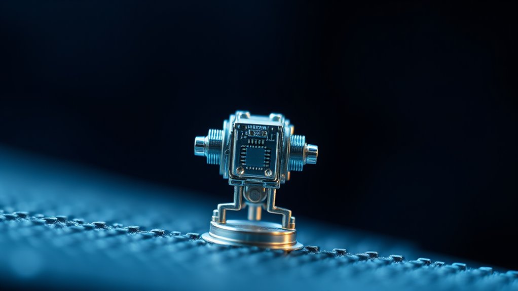
The Guinness World Record for the smallest medical robot is held by a 120-nanometer magnetoelectric nanorobot. This tiny device features a core–shell structure made of cobalt ferrite and barium titanate, enabling it to change shape and move using magneto-elasto-electric coupling. You can remotely control its locomotion, making it capable of interacting with cells and potentially delivering drugs inside cells. Fabricating such a nanorobot took two years, involving complex processes to develop and customize the core–shell nanocomposites at this incredibly small scale. Its size is much smaller than dust particles and comparable to large biomolecules, making it invisible to the naked eye. This breakthrough represents a significant step forward in medical nanorobotics, opening new possibilities for minimally invasive treatments. Innovative nanotechnology is driving the development of these miniature devices, highlighting the potential for further advancements in healthcare.

SwitchBot Universal Remote Control with Hub 3
【Effortless Control for All Your Devices】Easily manage your home’s infrared appliances such as air conditioners, TVs, fans, lights,…
As an affiliate, we earn on qualifying purchases.
As an affiliate, we earn on qualifying purchases.
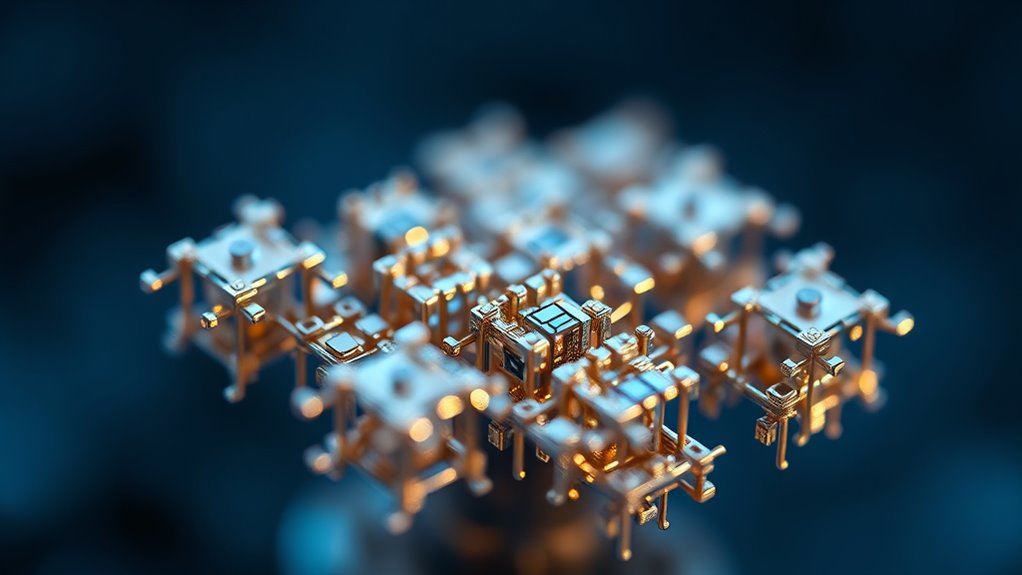
Advances in Microrobots: From Microns to Nanometers
Recent breakthroughs have pushed the boundaries of microrobotics, shrinking devices from the micron scale down to nanometers. You now can explore nanorobots with remarkable capabilities, including intracellular drug delivery and precise cell manipulation. Advances include:
Recent breakthroughs have miniaturized microrobots to nanometer scales, enabling precise cellular manipulation and advanced biomedical applications.
- Medical nanorobots as small as 120 nm, capable of shape change and locomotion via magneto-electric coupling.
- Walking microrobots down to 2–5 microns, using patterned nanomagnets and magnetic fields for controlled movement.
- Nanoscale logic devices under 50 nm, enabling in-body control and ultradense computing.
- Nano‑LEDs and nanopixels smaller than 200 nm, supporting high-density displays and near-field optical effects.
- Nanolasers and sensors, with sizes reaching just a few nanometers for integrated photonics and molecular detection.
These innovations mark a new era where microrobots become more versatile, precise, and integrated than ever before.
ultracompact nanolasers
As an affiliate, we earn on qualifying purchases.
As an affiliate, we earn on qualifying purchases.
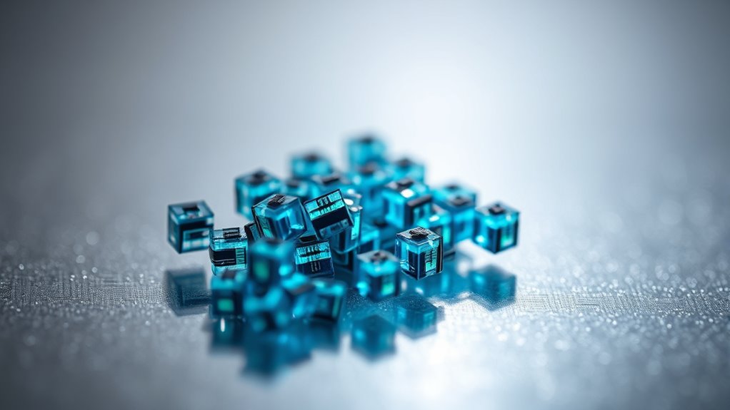
Pushing the Limits of Nanoscale Computing Devices

You’ll face significant fabrication challenges as you push nanoscale computing devices below 50 nm, where current manufacturing methods struggle with reliability and consistency. To overcome these limits, researchers are exploring unconventional logic approaches, such as memristive elements, that operate at molecular scales. These tiny devices hold promise for in-body applications like targeted control of nanobots and real-time sensing within biological tissues. Additionally, advances in AI-enabled design are helping to optimize fabrication processes at the nanoscale, potentially improving device reliability and scalability. As the development of ethnic diversity continues, understanding the varied backgrounds of researchers can foster more inclusive innovation in nanotechnology. Moreover, ongoing research into molecular manufacturing aims to revolutionize how nanoscale devices are produced, enhancing precision and efficiency in fabrication processes.
Fabrication Challenges Ahead
Pushing the limits of nanoscale computing devices faces significant fabrication challenges that hinder their practical deployment. Achieving reliable, precise structures at sub-50 nm scales pushes current manufacturing methods beyond their limits. You’ll encounter obstacles like:
- Difficulties in creating uniform, defect-free layers for stacked nanomemristors and logic elements
- Challenges in aligning nanoscale components with high accuracy
- Limitations of current lithography techniques for three-dimensional, densely packed architectures
- Thermal and electrical stability issues due to extreme miniaturization
- Material variability and reliability concerns over device lifespan
- Advancements in nanofabrication are essential to develop innovative techniques capable of overcoming these issues and enabling mass production. Progress in nanomanufacturing techniques could provide solutions to some of these fabrication hurdles.
Overcoming these hurdles demands advancements in nanofabrication, novel materials, and innovative assembly methods. Without these improvements, realizing the full potential of nanoscale logic devices remains a significant obstacle on the path to ultra-dense, efficient computing systems.
Unconventional Logic Approaches
To overcome the fabrication hurdles that limit traditional nanoscale logic devices, researchers are exploring unconventional approaches that leverage novel materials and architectures. Instead of relying solely on silicon-based components, they experiment with memristors, nanomagnetic elements, and molecular switches to create logic functions. These systems harness quantum effects, phase changes, or electrical resistance states at atomic scales, enabling logic operations within tiny footprints. By stacking layers or integrating multiple functionalities in a single nanostructure, they push beyond the limits of conventional lithography. These approaches allow for ultradense, energy-efficient computation, essential for in-body applications and complex nanosystems. Although challenges remain in reliability and control, unconventional logic architectures open new pathways for truly miniature, versatile, and scalable nanoscale computing devices.
Potential In-Body Applications
Advancements in nanoscale computing devices open exciting possibilities for in-body applications by enabling ultra-compact, intelligent systems that can operate within biological environments. You could deploy tiny nanorobots for targeted drug delivery, precise cell manipulation, or real-time electrical sensing. These devices can navigate complex tissues, interact with specific cells, and perform tasks with minimal invasiveness. Potential applications include:
- Delivering medication directly into affected cells
- Monitoring biochemical signals in real time
- Manipulating cell behavior for therapies
- Detecting early disease markers
- Assisting in minimally invasive surgeries
nanosensors for biomedical use
As an affiliate, we earn on qualifying purchases.
As an affiliate, we earn on qualifying purchases.
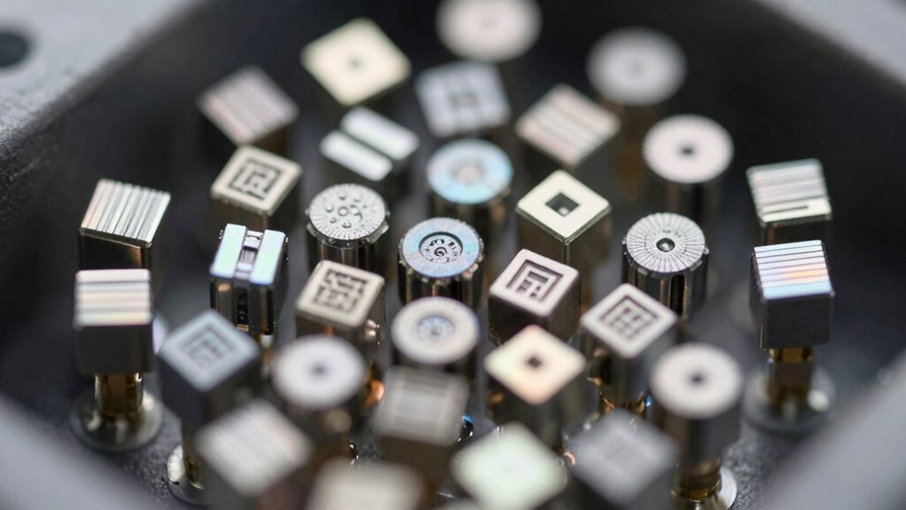
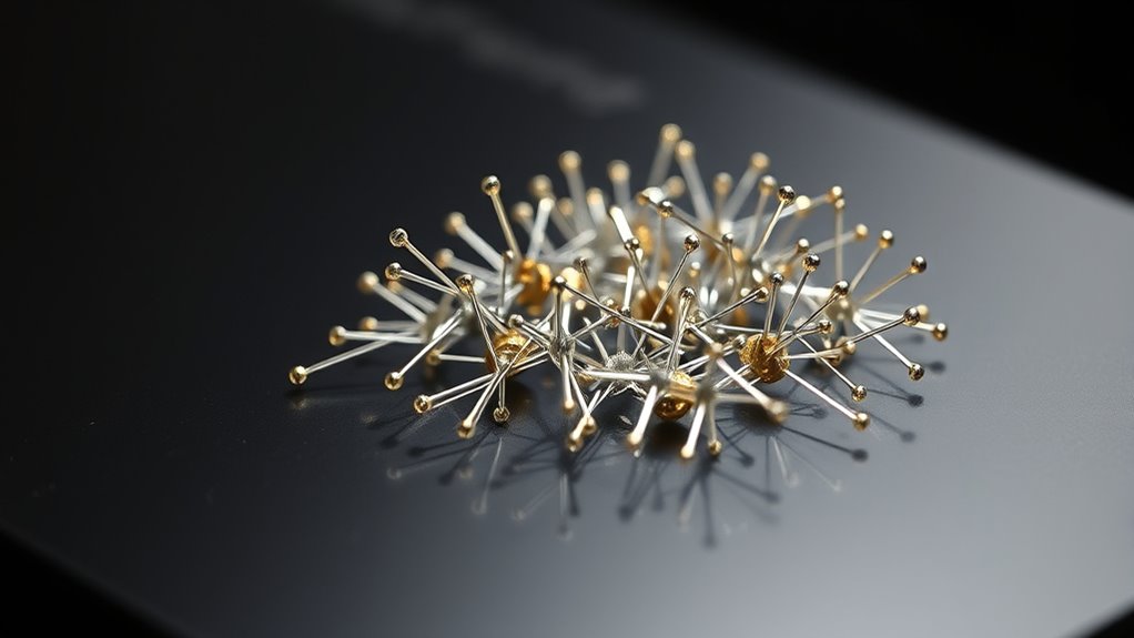
Breakthroughs in Nanoscale Light Sources and Pixels
Have you ever wondered how tiny light sources are revolutionizing nanotechnology? Recent breakthroughs have pushed pixel sizes below 100 nanometers, enabling ultra-dense displays and integrated photonic systems. ETH Zurich developed nano-LEDs with pixel diameters around 100 nm, increasing pixel density by thousands of times. Würzburg’s active nanopixels, just 300×300 nm, operate efficiently under ambient conditions for weeks. Nano‑PeLEDs achieve lengths near 90 nm, reaching over 127,000 pixels per square millimeter. These pixel sizes are below the diffraction limit for visible light, allowing near-field optical interactions and novel wave effects. Importantly, fabrication techniques now align with standard lithography processes, supporting scalable semiconductor integration. The development of nanoscale fabrication techniques has played a crucial role in enabling these cutting-edge devices. These advancements open new possibilities for high-resolution imaging, on-chip optical communication, and compact display technologies, all at an unprecedented nanoscale.
Innovations in Ultracompact Nanolasers for Photonic Integration
You can see how size reduction techniques have pushed nanolasers to nanometer scales, enabling integration directly onto chips. Improving on-chip light efficiency remains a key challenge, as smaller active volumes tend to increase thresholds and heat management issues. These innovations open up new applications in photonics, from high-density interconnects to compact sensing systems. Auditory processing considerations are crucial in designing these tiny devices to ensure optimal performance and reliability.
Size Reduction Techniques
Size reduction techniques for ultracompact nanolasers have become essential to meet the growing demand for dense photonic integration on chips. You can achieve this by employing plasmonic resonators, which confine light at subwavelength scales, or using dielectric nanostructures that minimize losses while shrinking device size. Incorporating quantum dots or nanowire gain media allows for highly localized amplification within tiny footprints. Techniques like top-down lithography and self-assembly enable precise nanoscale patterning and reproducibility. Additionally, hybrid approaches combine different materials to optimize performance and reduce active volumes. These innovations help overcome thermal and coupling challenges, making nanolasers smaller, more efficient, and suitable for integration into complex photonic circuits.
- Plasmonic and dielectric resonators for tight confinement
- Quantum dot and nanowire gain media integration
- Advanced lithography and self-assembly techniques
- Hybrid material approaches for performance optimization
- Thermal and coupling management at nanoscale
On-Chip Light Efficiency
Advancements in on-chip nanolasers focus on maximizing light efficiency to meet the demands of dense photonic integration. Researchers develop ultracompact lasers using plasmonic and dielectric resonators, which enhance light confinement at nanometer scales. These innovations reduce active volumes, lowering power thresholds and improving energy efficiency. By engineering gain media at the nanoscale, you can achieve higher emission rates and better coupling with waveguides, increasing overall output. Material choices like III-V semiconductors, perovskites, and hybrid structures play a critical role in optimizing performance. Thermal management remains a challenge, but recent designs incorporate heat sinks and novel cooling techniques. The goal is to produce reliable, low-threshold nanolasers that seamlessly integrate with existing photonic circuits, enabling high-density, energy-efficient optical interconnects on chips. Material optimization is essential for enhancing the performance and durability of these nanoscale devices. Furthermore, ongoing research into Thermal management strategies continues to drive progress toward more robust and long-lasting nanolasers, with innovations in heat dissipation techniques contributing to improved device stability.
Applications in Photonics
How are ultracompact nanolasers transforming photonic integration? These tiny lasers enable unprecedented miniaturization and performance in optical circuits. They fit into chip-scale environments, reducing size and power consumption while increasing integration density. Their small active volume boosts energy efficiency and allows for dense packing on photonic chips. With innovative fabrication techniques, nanolasers now use plasmonic or dielectric resonators to sustain lasing at nanometer scales. This advances applications like high-speed data transfer, on-chip sensing, and quantum computing. You’ll find that these nanolasers support complex functionalities, including:
- On-chip optical interconnects
- Dense photonic circuitry
- Low-threshold laser sources
- Integrated sensors and detectors
- Energy-efficient photonic systems
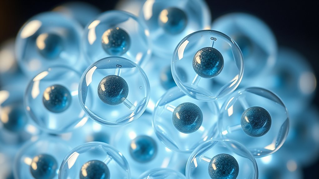
Developing Nanoscale Sensors for Cellular and Molecular Monitoring
Developing nanoscale sensors for cellular and molecular monitoring is revolutionizing how you observe biological processes at the smallest scales. These sensors, often just tens of nanometers, enable real-time detection of electrical, optical, and magnetic signals within single cells or molecules. By integrating materials like plasmonic metals or ferroelectric composites, you gain high sensitivity and specificity. You can measure forces, fields, or chemical concentrations directly at the cellular level, providing insights into disease mechanisms, drug interactions, and cellular functions. Advances in fabrication now allow these sensors to operate reliably over extended periods, with stability and efficiency improvements. As a result, you’re able to perform non-invasive, highly localized measurements that were previously impossible, opening new frontiers in biomedical research and personalized medicine.
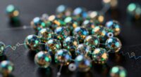
Fabrication Challenges of Sub-Micron Core–Shell Nanocomposites
Fabricating sub-micron core–shell nanocomposites presents significant technical hurdles because achieving precise control over their nanoscale architecture demands advanced synthesis techniques. You need to manage uniform shell thickness, prevent aggregation, and guarantee consistent core-shell interfaces. Challenges include:
- Achieving nanometer-scale precision during deposition
- Controlling material interface quality
- Preventing shell defects and discontinuities
- Maintaining stability during synthesis
- Scaling up production without losing uniformity
These issues require sophisticated methods like atomic layer deposition, chemical vapor deposition, or templating techniques. nanoscale control is crucial for ensuring the desired properties of the final product. Additionally, developing scalable fabrication methods remains a key hurdle for commercial applications. Overcoming these challenges is essential to unlock the full potential of core–shell nanocomposites, especially when integrating advanced materials for innovative applications. Moreover, a thorough understanding of surface chemistry is vital to optimize interfacial interactions and improve overall synthesis success. Advances in precise deposition techniques are also critical to achieving consistent nanoscale features.
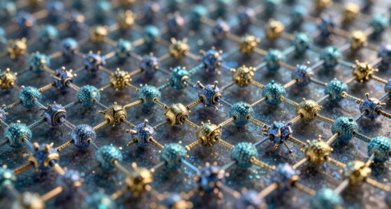
Magnetic Patterning and Actuation at the Nanoscale

You can achieve precise magnetic patterning at the nanoscale using advanced lithography and self-assembly techniques, enabling detailed control over magnetic domains. Nanoscale magnetic actuation strategies leverage external magnetic fields and patterned nanomagnets to drive motion and shape changes in tiny devices. By combining these methods, researchers can create highly responsive nanomachines capable of complex tasks within biological and technological environments. The development of vetted Vetted flat iron bikes demonstrates the practical application of reliable and efficient electric components in modern transportation. Additionally, recent advancements in magnetic materials have enhanced the stability and responsiveness of nanoscale magnetic systems, further expanding their potential applications.
Precise Magnetic Patterning Techniques
Precise magnetic patterning at the nanoscale leverages advanced lithography, deposition, and etching techniques to create highly controlled magnetic structures with nanometer resolution. You can manipulate magnetic domains and tailor magnetic properties with great accuracy. Techniques like electron-beam lithography enable patterning features just a few nanometers wide. Focused ion beam (FIB) milling allows direct sculpting of magnetic materials. Atomic layer deposition (ALD) offers uniform thin films for complex patterns. Self-assembly processes guide nanoscale magnetic structures without direct patterning. These methods facilitate the fabrication of nanoscale magnetic sensors, actuators, and memory devices. Advanced fabrication techniques play a crucial role in achieving the precision required for these tiny devices.
Nanoscale Magnetic Actuation Strategies
Nanoscale magnetic actuation strategies harness advanced patterning techniques and external magnetic fields to control the movement and behavior of tiny devices with nanometer precision. You can manipulate magnetic nanostructures to induce shape changes, steer nanorobots, and activate functionalities remotely. These strategies rely on precise magnetic patterning, enabling localized control over individual components. External fields then drive motion, allowing for targeted drug delivery, cell manipulation, or sensing within biological tissues. The combination of patterning and external fields release dynamic control at an unprecedented scale. Additionally, these techniques benefit from principles such as Free Floating, which facilitate versatile and adaptable device operation without physical constraints.
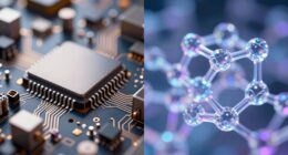
Material Systems Powering Next-Generation Nanoscale Devices
What materials enable the extraordinary miniaturization of next-generation nanoscale devices? You’ll find that advanced composites, semiconductors, and metals drive innovation. These materials offer unique properties suited for nanoscale applications, such as high electrical conductivity, ferroelectricity, and magnetic responsiveness. Key materials include:
Advanced composites, semiconductors, and metals enable the miniaturization of next-generation nanoscale devices.
- Core–shell ferroelectric/magnetic composites for nanorobots
- Organic semiconductors enabling flexible nanosensors
- Plasmonic metals like gold and silver for nano‑light sources
- Dielectric nanoparticles for ultracompact lasers
- Memristive oxides used in nanoscale logic devices
These materials allow for precise control, miniaturization, and multifunctionality. They also facilitate fabrication techniques compatible with existing semiconductor processes, supporting the integration of complex nanosystems. Material properties are critical in enabling the diverse functionalities required at the nanoscale. Their versatility underpins many breakthroughs in miniaturized devices, pushing the boundaries of what’s possible at the nanoscale.
Future Perspectives on the Miniaturization of Machines
As advancements in materials and fabrication techniques continue, the miniaturization of machines is poised to reach unprecedented levels, opening new horizons for applications in medicine, computing, and sensing. You’ll see nanomachines capable of performing complex tasks inside the human body, like targeted drug delivery or cellular repair, with minimal invasiveness. Computing elements will shrink below 50 nm, enabling ultradense, energy-efficient processors integrated directly into biological systems. Light sources and sensors will become even smaller, allowing real-time monitoring at cellular scales. Future devices will utilize novel materials like plasmonics and ferroelectric composites to enhance performance and stability. Additionally, innovations in nanofabrication techniques will allow for more precise and scalable production of these tiny machines, accelerating their integration into various fields. As these tiny machines evolve, you’ll witness a convergence of nanotechnology, biotechnology, and photonics, unlocking possibilities that transform healthcare, communication, and environmental sensing.
Frequently Asked Questions
How Do Nanoscale Devices Maintain Stability and Reliability Over Time?
You guarantee nanoscale devices maintain stability and reliability by selecting robust materials like ferroelectric/magnetic composites, organic semiconductors, or plasmonic metals. You optimize fabrication processes to minimize defects and filament formation, and implement protective coatings to guard against environmental factors. Regular calibration, efficient thermal management, and ongoing research into long-term operation help you improve durability, prevent degradation, and extend the functional lifespan of your nanoscale devices.
What Are the Main Technical Hurdles in Fabricating Sub-50 Nm Nanodevices?
You face major challenges in fabricating sub-50 nm nanodevices, mainly due to limitations in current lithography and nanofabrication techniques that struggle with precision and reproducibility at such tiny scales. Controlling defects, ensuring consistent material properties, and managing quantum effects are tough. Additionally, integrating multiple layers and maintaining device stability over time require advanced processes, which are still under active development.
How Do Nanoscale Robots Achieve Precise Control Within Biological Tissues?
You can control nanoscale robots in biological tissues through external stimuli like magnetic fields, electrical signals, or light. These stimuli induce shape changes, movement, or sensing capabilities. Precise control depends on advanced fabrication to incorporate responsive materials, accurate external actuation methods, and real-time feedback systems. By tuning these elements, you guarantee the nanorobots interact accurately with cellular environments, enabling targeted drug delivery, cell manipulation, or localized sensing.
What Materials Enable Both High Efficiency and Durability in Ultracompact Light Sources?
You’ll find that plasmonic metals, organic semiconductors, and dielectric materials are key for high-efficiency, durable ultracompact light sources. For example, nano-LEDs and nanopixels with sizes below 100 nanometers can achieve remarkable pixel densities, like 127,000 per mm². These materials enable near-field interactions and stable operation under ambient conditions, making them ideal for integration into compact photonic devices that demand both longevity and performance.
How Close Are We to Integrating These Tiny Devices Into Practical Medical Applications?
You’re getting close to integrating these tiny devices into practical medical applications. Advances in nanomaterial fabrication, precise targeting, and control methods are making it possible to develop nanorobots for drug delivery, cell manipulation, and localized sensing. While challenges remain—like ensuring stability, biocompatibility, and reliable operation—you’ll see increasing use in diagnostics, minimally invasive treatments, and personalized medicine in the near future as research continues to progress.
Conclusion
You’ve seen how researchers have pushed the boundaries, creating devices as small as a few nanometers. Did you know the smallest medical robot is only 1.5 microns long? This incredible miniaturization releases potential for targeted treatments and advanced tech. As scientists continue shrinking machines, the future promises even more astonishing innovations, transforming medicine, computing, and beyond. Keep an eye on these tiny marvels—they’re changing our world one nanometer at a time.