
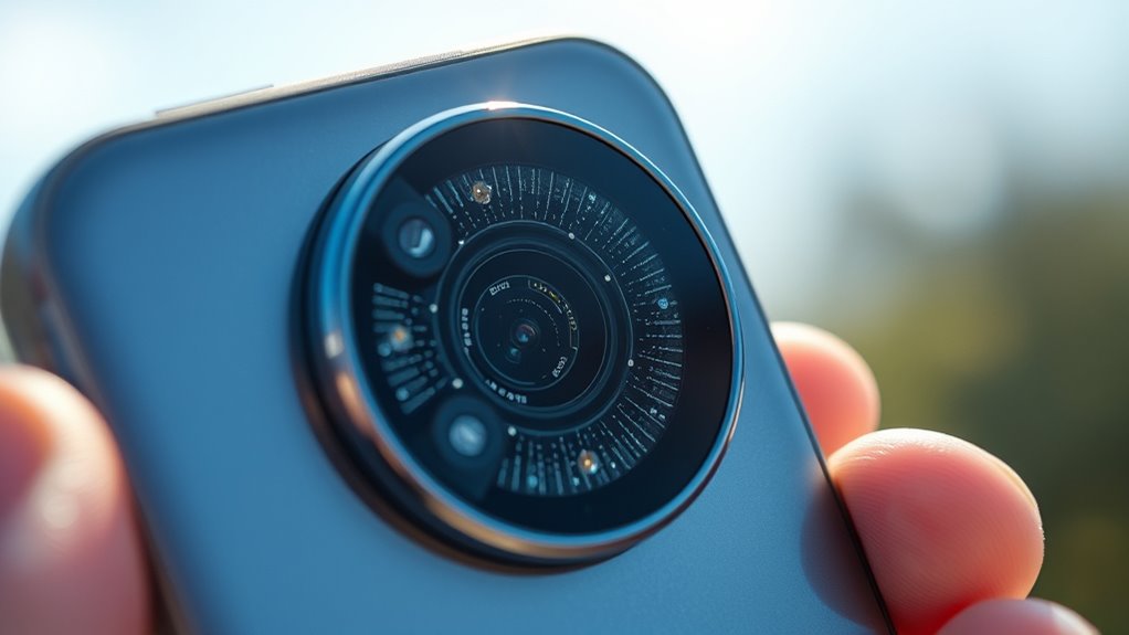
Nanotech inside your smartphone camera uses tiny structures like nanoprism lenses, metasurfaces, and advanced materials to manipulate light precisely. These innovations boost photon capture, reduce optical losses, and support ultra-thin, sleek designs. They also improve low-light performance, color accuracy, and detail. Scalable nanofabrication guarantees these components are high quality and durable. By combining nanotech with AI and computational imaging, your photos become clearer and more vibrant—discover how these tiny tech tricks make a big difference.
Key Takeaways
- Nanostructured optical components enhance light capture and reduce losses, resulting in brighter, clearer photos.
- Ultra-thin metasurfaces and metalenses precisely shape wavefronts for sharper images within compact camera modules.
- Nanomaterials and coatings improve environmental resistance, minimize reflections, and boost low-light performance.
- Advanced nanofabrication enables high-resolution sensors with features like polarization sensitivity and multi-spectral imaging.
- These nanoscale innovations support better image processing, reducing noise and enhancing detail in every shot.

Xenvo Pro Lens Kit for iPhone and Android, Macro and Wide Angle Lens with LED Light and Travel Case Black
✔ COMPATIBLE WITH ALL SMARTPHONES, TABLETS, and LAPTOPS including ALL iPhone models, Samsung Galaxy and Note, Google Pixel,…
As an affiliate, we earn on qualifying purchases.
As an affiliate, we earn on qualifying purchases.
How Nanoprism Light Guides Boost Low-Light Performance

Nanoprism light-guiding layers enhance low-light performance by increasing the amount of photons captured by each pixel. These nanostructures use tiny prismatic microlenses to funnel incoming light directly into the photodiodes, reducing optical losses from shallow-angle rays. As a result, more light reaches your sensor without enlarging pixel size, boosting sensitivity in dim environments. This improved photon collection means your images have less noise and better detail in low-light conditions. Because the nanoprism layers are integrated into the microlens stacks, they preserve the sensor’s compact form factor, enabling higher megapixel counts—like 200 MP sensors—while maintaining small pixel sizes. Additionally, the nanoprism structures are designed to minimize optical distortions that can occur with complex light paths. These advancements are supported by innovative manufacturing techniques, which ensure precise nanostructure fabrication and consistent performance. Furthermore, ongoing research into advanced materials is expected to further enhance the durability and efficiency of these nanostructures. Incorporating light management strategies helps optimize the overall sensor performance and image quality. Ultimately, this technology allows you to take clearer, brighter photos at night or in challenging lighting, all without sacrificing your device’s slim profile. Innovative European cloud servers support the development of advanced sensor technologies by providing sustainable and secure data infrastructure, fostering ongoing innovation in mobile imaging.
metasurface smartphone camera module
As an affiliate, we earn on qualifying purchases.
As an affiliate, we earn on qualifying purchases.
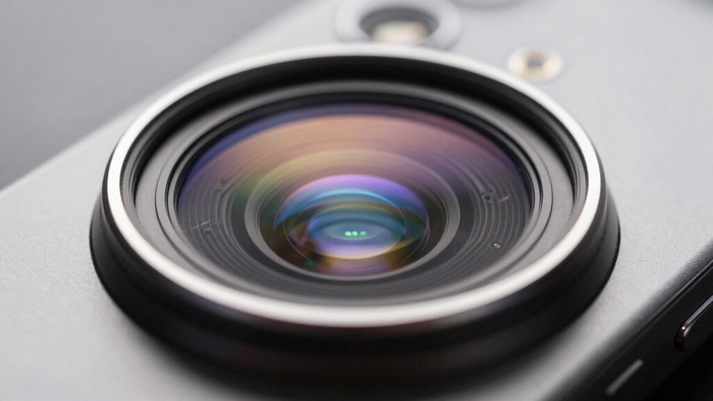
Metasurfaces and Metalenses: The Future of Compact Optics
Metasurfaces and metalenses make optics ultra-thin and lightweight, fitting complex functions into micrometer-thin layers. They shape wavefronts with high precision, replacing bulky traditional lenses and enabling new device form factors. Thanks to integrated manufacturing processes, these components can be produced at scale, reducing costs and opening the door to innovative smartphone designs. Advanced manufacturing techniques further enhance the scalability and affordability of these optical components. Additionally, these technologies support environmental considerations by enabling more sustainable manufacturing practices. Their precise wavefront control also allows for miniaturization of optical systems, making devices more portable and versatile. Moreover, the development of mass production methods ensures consistent quality and facilitates widespread adoption in consumer electronics. Ensuring compatibility with various body jewelry materials can also improve the durability and performance of integrated optical components.
Ultra-thin Optical Components
Advances in flat optics are transforming smartphone cameras by replacing bulky curved lenses with ultra-thin metasurfaces and metalenses. These nanostructured components are just a few micrometers thick, yet they can focus light, correct aberrations, and manage dispersion—functions once requiring multiple glass elements. By using subwavelength nanoposts or antennas, metasurfaces shape wavefronts directly on a flat surface, drastically reducing camera size. This allows manufacturers to create slimmer devices, with some designs integrating entire imaging systems into a single, flat layer. Metalenses and metasurfaces also enable new form factors, like conformal or surface-mounted cameras, while maintaining optical performance. Their compactness and manufacturing compatibility with semiconductor processes promise cost-effective production and innovative device designs, shaping the future of high-quality, miniaturized smartphone optics.
Wavefront Shaping Precision
By manipulating wavefronts directly on a flat surface, metasurfaces and metalenses enable precise control over light focusing, dispersion, and aberration correction in ultra-thin layers. This wavefront shaping precision allows your smartphone camera to achieve high-quality images without bulky lenses. Nanoposts and nanoantennas tune phase and amplitude at subwavelength scales, correcting distortions and expanding the field of view. The following table highlights key advantages:
| Key Feature | Benefit | Application |
|---|---|---|
| Subwavelength control | Precise wavefront manipulation | High-resolution focusing |
| Aberration correction | Clear, sharp images in various conditions | Night and low-light photography |
| Compact design | Slimmer devices, new form factors | Thinner smartphones |
This technology enables advanced, compact optics, transforming your camera experience.
Integrated Manufacturing Benefits
How does integrated manufacturing revolutionize the production of nanoscale optical components? It allows you to mass-produce complex metasurfaces and metalenses with high precision using semiconductor fabrication techniques like lithography and wafer-scale patterning. This approach reduces costs, speeds up production, and guarantees consistent quality across billions of units. You can embed nanoscale optics directly into device surfaces or stack layers within tight form factors, enabling thinner, lighter cameras without sacrificing performance. Integrated manufacturing also supports scalable, reliable assembly of advanced coatings, dielectric nanopillars, and interconnects, improving durability and image quality. Additionally, understanding reliability and safety concepts in manufacturing can help optimize the design for better performance. By streamlining fabrication, this method accelerates innovation, making sophisticated nanophotonic elements affordable and accessible for consumer electronics, ultimately transforming your smartphone’s camera capabilities. Moreover, advancements in quality control during manufacturing ensure each component meets strict standards, further enhancing device reliability.
Xenvo Pro Lens Kit for iPhone and Android, Macro and Wide Angle Lens with LED Light and Travel Case Black
✔ COMPATIBLE WITH ALL SMARTPHONES, TABLETS, and LAPTOPS including ALL iPhone models, Samsung Galaxy and Note, Google Pixel,…
As an affiliate, we earn on qualifying purchases.
As an affiliate, we earn on qualifying purchases.
Advanced Materials and Nanofabrication for Smartphone Cameras

You can take advantage of nano-structured optical layers made from materials like silicon dioxide and titanium dioxide, which precisely control light at the smallest scales. Advanced nanofabrication techniques, such as high-precision lithography, enable the creation of these complex structures with sub-10 nanometer accuracy. By combining innovative materials with these precise manufacturing methods, smartphone cameras become more efficient, compact, and capable of capturing higher-quality images in challenging conditions. This integration of nanotechnology significantly enhances the optical performance and opens new possibilities for future camera innovations. Moreover, understanding quantum effects at the nanoscale can further improve light manipulation and image quality in next-generation devices. As research progresses, developing advanced materials tailored for specific optical functions could revolutionize mobile imaging even further, paving the way for more miniaturized optical components that fit seamlessly into compact devices. Additionally, exploring novel fabrication techniques can lead to even finer control over nanoscale structures, pushing the boundaries of optical performance.
Nano-structured Optical Layers
Nano-structured optical layers are transforming smartphone cameras by leveraging advanced materials and nanofabrication techniques to enhance light management and image quality. These layers include nanoprism microlenses that boost light absorption by about 25%, improving low-light sensitivity without increasing pixel size. Nano-funnels bend incoming rays into photodiodes, reducing optical loss and increasing signal clarity in dim scenes. Metasurfaces and metalenses replace bulky curved optics with flat, ultra-thin layers that focus, correct aberrations, and control dispersion, all within micrometers. High-precision fabrication of dielectric nanopillars and nano-coatings reduces reflections, contamination, and enhances contrast. These nano-structures enable better photon capture, lower noise, and higher dynamic range, delivering clearer images in challenging lighting conditions and maintaining the compact form factor of modern smartphones. Additionally, nanofabrication techniques allow for precise manipulation of light at the nanoscale, further enhancing the overall performance of these optical layers.
Precision Nanofabrication Techniques
Advanced materials and nanofabrication techniques are revolutionizing the manufacturing of smartphone camera components by enabling the precise creation of nanoscale structures with remarkable consistency. These methods allow you to produce intricate features like nanoprism layers, metasurfaces, and nanopillars that enhance light collection, focus, and image quality. Techniques such as electron-beam lithography, atomic layer deposition, and wafer-scale patterning ensure sub-10 nm tolerances, vital for uniform performance across millions of sensors. This precision supports the integration of complex optical elements directly onto chips, reducing size and weight while boosting sensitivity. Nanomanufacturing ensures these complex structures can be produced efficiently at scale.
ultra-thin metalens for smartphones
As an affiliate, we earn on qualifying purchases.
As an affiliate, we earn on qualifying purchases.
The Role of Computational Imaging and AI in Enhancing Photos
Computational imaging and AI are transforming smartphone photography by turning complex optical data into stunning, high-quality images. You benefit from algorithms that process raw sensor signals, correcting aberrations, reducing noise, and boosting detail. AI-driven techniques like machine learning help reconstruct images with enhanced clarity, color accuracy, and dynamic range, even in challenging lighting. When capturing low-light scenes, nanotech-enhanced photon capture feeds better data into these algorithms, resulting in cleaner images with less noise. Additionally, real-time computational features like HDR fusion, super-resolution, and digital zoom extend your device’s capabilities beyond traditional optics. By co-designing nanostructured optics with advanced algorithms, manufacturers create smarter sensors that produce crisp, vibrant photos without bulky lenses, making your smartphone’s camera more powerful and versatile every year.
Pushing the Limits of Sensor Size and Megapixels With Nanotech
By leveraging nanotech innovations, smartphone sensors can achieve unprecedented megapixel counts without sacrificing sensitivity or image quality. Nanoprism light-guiding layers enhance photon absorption by about 25%, boosting low-light performance without increasing pixel size. These nanostructures enable high-megapixel sensors, like 200 MP, while maintaining small pixel dimensions, preserving sensor compactness. Nano-scale prismatic funnels direct incoming rays into photodiodes, reducing optical loss and improving signal-to-noise ratios in dim scenes. Additionally, nanotech coatings and materials improve light throughput, lowering ISO requirements and reducing noise. This allows for clearer images even in challenging lighting. Furthermore, sensor efficiency improvements driven by nanotech enable more power-efficient operation and longer battery life for smartphones. Overall, nanotechnology pushes the boundaries of sensor size and resolution, delivering crisper, more detailed photos without compromising sensitivity or device form factor.
Transforming Device Design: Slimmer, Smarter, and More Robust Cameras

Nanotech innovations are revolutionizing device design by enabling thinner, more durable smartphone cameras that don’t compromise on performance. Metasurfaces and metalenses replace bulky optics, allowing for ultra-flat, lightweight modules with excellent focusing and aberration correction. These nanostructures enable the creation of slim, conformal cameras that can be integrated across device surfaces, eliminating traditional bumps and reducing weight. Advanced nanomaterials and coatings enhance durability, resistance to moisture, and environmental stress, ensuring longer-lasting performance. High-precision nanofabrication maintains consistent optical quality while supporting complex designs. As a result, your smartphone can become sleeker yet more powerful, with robust construction that withstands daily wear. This synergy of nanotech and design pushes the boundaries of compactness, durability, and smarter functionality in modern device engineering.
Real-World Benefits: Better Night Shots and Dynamic Range

Nanostructured optical components inside smartphone cameras substantially enhance night photography and dynamic range. These nanotech features, like nanoprism light-guiding layers, improve photon capture in low-light conditions, reducing noise and increasing image clarity. They direct more light into photodiodes, boosting sensitivity without enlarging pixels. This integration of nanotechnology allows for more precise control of light at the microscopic level, leading to better image quality. This means your night shots are brighter, clearer, and have better detail. Additionally, these nanostructures expand the dynamic range, capturing both shadows and highlights more effectively. By utilizing advanced nanotechnology, smartphone cameras can deliver significantly improved image quality in various lighting environments. These innovations involve light manipulation at the nanoscale, enabling more efficient light management within the sensor. The use of nanostructures also enables manufacturers to create more compact camera modules with enhanced performance. Here’s how they make a difference:
| Benefit | Explanation |
|---|---|
| Increased sensitivity | More light reaches the sensor, improving low-light photos |
| Reduced noise | Higher photon capture results in cleaner images |
| Better contrast | Enhanced dynamic range captures full scene detail |
| Sharper night shots | Overall, images are clearer and more vibrant |
These advances let you take stunning photos even in challenging lighting.
Looking Ahead: Next-Gen Imaging With Nanoscale Innovations

Advances in nanoscale imaging components are paving the way for smartphones to achieve unprecedented levels of performance. Future designs will incorporate ultra-thin metalenses and metasurfaces that replace bulky optics, enabling compact, lightweight devices with broader fields of view and improved image quality. These nano-engineered lenses work seamlessly with computational algorithms, allowing for real-time correction of aberrations and enhanced resolution. Nanoscale materials and coatings will further boost sensor efficiency, reduce noise, and enable new functionalities like polarization sensitivity and multi-spectral imaging. As manufacturing processes become more scalable, expect smartphones to feature fully integrated, surface-mounted nanoscale imagers that eliminate camera bumps and support innovative form factors. These innovations will drastically improve low-light performance, dynamic range, and computational photography, transforming what your device can capture.
Frequently Asked Questions
How Do Nanostructures Improve Image Quality Without Increasing Pixel Size?
Nanostructures boost image quality by increasing light absorption and directing incoming rays more efficiently into your camera’s photodiodes. This means you get better low-light sensitivity and less noise without enlarging pixels. They also help shape wavefronts for sharper focus and reduce optical losses, so your photos look clearer and brighter even in dim conditions. Plus, their compact design keeps your device slim while delivering high-quality images.
Can Metasurfaces Enable Fully Flexible or Wearable Camera Systems?
Metasurfaces are like a flexible fabric, capable of conforming to various shapes, which makes fully wearable camera systems possible. They can be integrated onto curved or uneven surfaces, enabling cameras that bend and flex with your movements. Their ultra-thin, lightweight design means you can embed them into clothing, glasses, or even skin-like patches. This flexibility opens the door to seamless, unobtrusive imaging devices that adapt to your lifestyle and environment.
What Materials Are Most Commonly Used in Nanofabrication for Smartphone Optics?
You’ll find silicon dioxide and titanium dioxide are most commonly used in nanofabrication for smartphone optics. These high-refractive-index dielectric materials form nanoscale pillars and phase-shifting elements that control light precisely. They’re favored because they offer excellent optical performance, are compatible with wafer-scale manufacturing, and provide durability. Additionally, materials like nano-coatings, anti-reflective films, and nanocomposites enhance contrast, reduce reflections, and protect delicate components, ensuring your camera performs reliably in real-world conditions.
How Do Nanotech Enhancements Affect Manufacturing Costs and Scalability?
Imagine turning a tiny, fragile toy into a resilient robot—nanotech makes this possible for manufacturing. These enhancements, like wafer-scale patterning and high-precision lithography, initially raise costs but scale efficiently as production ramps up. You benefit from reduced long-term expenses thanks to streamlined processes, fewer bulky parts, and smaller, more integrated components. Over time, nanotech’s scalability helps lower prices, making advanced smartphone cameras accessible to everyone.
Will Nanostructured Optics Allow Smartphones to Capture Spectral or Depth Information?
Yes, nanostructured optics can enable your smartphone to capture spectral and depth information. By embedding nanoscale elements like metasurfaces and specialized nanophotonic structures, your device can encode additional scene data directly into the captured signals. This allows for features like precise depth sensing and spectral imaging, enhancing AR experiences and improving photo quality. As fabrication advances, expect more compact, integrated sensors that bring these capabilities seamlessly into your everyday smartphone.
Conclusion
With nanotech nurturing your night shots and boosting brilliance, your smartphone’s sensor sophistication soars. By blending breakthroughs in bots, beams, and boundaries, these tiny technologies transform your tech experience. As advancements accelerate, expect even more extraordinary images—brighter, bolder, and better than ever. Embrace the evolution, because the future of flawless photos is firmly fueled by fascinating, futuristic nanoscale innovations inside your device.