Nanotechnology enables you to create smaller, faster, and more energy-efficient chips and sensors by utilizing advanced materials like graphene, carbon nanotubes, and quantum dots. These innovations improve charge transport, boost processing speeds, and increase sensor sensitivity, driving miniaturization and enhanced performance in electronics. While integrating nanomaterials poses manufacturing challenges, ongoing progress points to a future with smarter, more versatile devices. Keep exploring to discover how these advancements are shaping next-generation electronics.
Key Takeaways
- Nanomaterials like graphene and carbon nanotubes enable smaller, faster, and more energy-efficient chips with increased transistor density.
- Nanoscale fabrication techniques such as electron beam lithography and atomic layer deposition allow precise patterning and ultra-thin film construction.
- Quantum dot technology enhances sensor sensitivity through size-dependent emission and quantum effects like tunneling and superposition.
- Integration of nanoscale transistors and nanostructures supports high-speed, miniaturized, and energy-efficient electronic devices.
- Challenges include ensuring manufacturing uniformity, handling toxicity concerns, and scaling nanotech processes for mass production.

Graphene Nanoelectronics: Metrology, Synthesis, Properties and Applications (NanoScience and Technology)
As an affiliate, we earn on qualifying purchases.
As an affiliate, we earn on qualifying purchases.
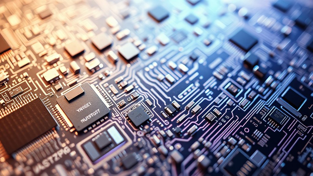
The Role of Nanomaterials in Chip Miniaturization

Nanomaterials have revolutionized chip miniaturization by enabling the creation of smaller, more efficient electronic components. You can now pack more transistors into a tiny space, boosting processing power without increasing size. These materials, such as carbon nanotubes and graphene, have exceptional electrical properties that outperform traditional silicon at small scales. By leveraging their unique characteristics, you can reduce the physical dimensions of components while maintaining or improving performance. This miniaturization allows for faster, more energy-efficient devices, paving the way for advanced smartphones, wearables, and IoT gadgets. As you work with nanomaterials, you’ll discover they open new possibilities for creating increasingly compact and powerful chips, ultimately transforming the landscape of modern electronics.

Ultrapure 95% Amino Modified Multi Walled Carbon Nanotubes Powder 8-15nm MWCNTs(5 Gram)
Product name: Amino modified MWCNT
As an affiliate, we earn on qualifying purchases.
As an affiliate, we earn on qualifying purchases.
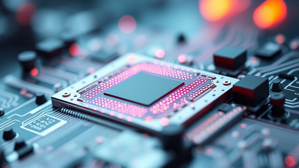
Enhancing Semiconductor Performance With Nanotech

Building on the advancements in chip miniaturization, nanotechnology offers powerful ways to boost semiconductor performance. By manipulating materials at the atomic level, you can reduce electron scattering, which improves speed and energy efficiency. Nanostructures like quantum dots and nanowires enhance charge transport, leading to faster switching times and lower power consumption. You can also engineer materials with tailored electronic properties, such as higher mobility or better thermal management. These improvements allow semiconductors to operate at higher frequencies and with greater reliability. Additionally, nanotech enables the creation of novel device architectures that optimize performance. As you integrate these nanomaterials, you’ll notice significant gains in processing power, energy efficiency, and device longevity—driving the next generation of high-performance electronics.

Quantum Dot Display Science and Technology (Wiley Series in Display Technology)
As an affiliate, we earn on qualifying purchases.
As an affiliate, we earn on qualifying purchases.
Nanoscale Fabrication Techniques for Electronics
Advancements in nanoscale fabrication techniques have revolutionized how you create electronic components with atomic precision. Techniques like atomic layer deposition allow you to build ultra-thin films layer by layer, ensuring exact thickness control. Electron beam lithography enables you to pattern features smaller than 10 nanometers, giving you exceptional detail for complex circuits. Focused ion beam milling lets you sculpt materials directly at the nanoscale, perfect for prototyping. Self-assembly processes guide molecules to form ordered structures without manual intervention, saving time and increasing uniformity. Understanding contrast ratio and other key display parameters helps optimize the performance of nanoscale electronic devices. These methods collectively improve device performance, reduce sizes, and enhance efficiency. As a result, you can develop faster, more powerful electronics with greater miniaturization, pushing the boundaries of what’s possible in modern semiconductor manufacturing.

Handbook of Thin Film Deposition
As an affiliate, we earn on qualifying purchases.
As an affiliate, we earn on qualifying purchases.
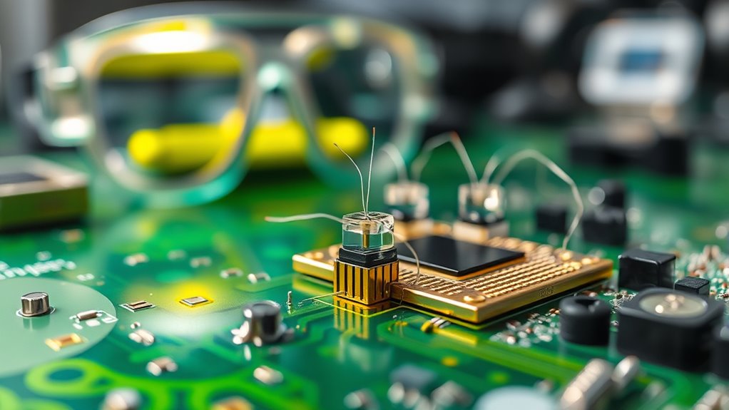
Quantum Dot Technology in Sensor Development
Quantum dot technology remarkably boosts sensor sensitivity, allowing you to detect even the smallest changes with greater accuracy. It also enables vibrant color display capabilities, making sensor readouts more vivid and easier to interpret. Exploring these features can lead to more responsive and visually engaging electronic devices.
Enhanced Sensitivity Features
Quantum dot technology has revolutionized sensor development by substantially enhancing sensitivity. By exploiting the unique quantum properties of nanocrystals, you can detect even trace amounts of chemicals, biological agents, or environmental changes with remarkable precision. This heightened sensitivity allows for early disease detection, pollution monitoring, and improved safety systems. Quantum dots improve signal clarity and reduce noise, making sensors more reliable and faster. The table below highlights key advantages:
| Feature | Benefit |
|---|---|
| Size-dependent emission | Precise tuning of detection wavelengths |
| High quantum yield | Strong, clear signals |
| Tunable properties | Customizable for specific applications |
| Brightness | Enhanced detection sensitivity |
| Stability | Consistent performance over time |
You now have the tools to develop ultra-sensitive sensors that meet the demands of modern technology. Nanocrystals’ unique quantum properties
Color Display Capabilities
Color display capabilities have been considerably enhanced by incorporating quantum dot technology, allowing for vivid, accurate, and customizable visuals. This advancement means you’ll see brighter colors, better contrast, and more precise color reproduction on screens. Quantum dots are tiny semiconductor particles that emit specific wavelengths of light when energized, resulting in richer and more vibrant displays. They also improve energy efficiency and extend device battery life. With quantum dot-enhanced displays, you get a more immersive viewing experience, whether for entertainment, professional work, or sensor feedback. You’ll notice sharper images and more consistent color accuracy across different viewing angles. This technology is revolutionizing how sensors and screens communicate data visually, making your devices smarter and more visually appealing. Additionally, quantum dot technology aligns with the principles of space efficiency, enabling more compact and versatile device designs without sacrificing performance.
Carbon Nanotubes and Graphene in Electronic Devices

Carbon nanotubes and graphene have revolutionized electronic device design by offering exceptional electrical, thermal, and mechanical properties. Their high conductivity and strength enable faster, more durable components, paving the way for ultra-thin, flexible electronics. You can now develop transistors with increased speed and efficiency, reducing power consumption. These materials also enhance sensor performance, improving sensitivity and stability. To illustrate their impact, consider this table:
| Property | Benefit |
|---|---|
| Electrical Conductivity | Faster data transmission |
| Mechanical Strength | Durable, flexible devices |
| Thermal Conductivity | Efficient heat dissipation |
| Light Weight | Portable, lightweight gadgets |
| Flexibility | Bendable, stretchable electronics |
Harnessing these materials takes your device innovation to a new level, making electronics smarter and more resilient. Vetted – Halloween Product Reviews
Improving Sensor Sensitivity Through Nanoscale Engineering

By engineering materials at the nanoscale, you can enhance sensor sensitivity through unique properties like increased surface area and altered electrical behavior. Optimizing surface interactions allows for more precise detection of target molecules, boosting overall performance. Additionally, leveraging quantum effects at this scale can markedly improve signal amplification and accuracy. Incorporating glycolic acid in surface treatments can further refine sensor responsiveness by promoting better material compatibility and reducing interference.
Nanoscale Material Properties
Have you ever wondered how nanoscale engineering enhances sensor performance? It all comes down to the unique properties of materials at the nanoscale. When materials shrink to nanometer sizes, their electrical, optical, and mechanical characteristics change dramatically, boosting sensor sensitivity. For example, nanomaterials can exhibit increased surface reactivity, quantum effects, and improved electron transport. These factors allow sensors to detect even trace amounts of chemicals, gases, or biological agents more accurately. By tailoring nanoscale material properties, you can optimize responsiveness, selectivity, and stability. Advancements in machine learning further support the design of these nanomaterials by predicting optimal structures and compositions for specific sensing applications.
Surface Area Optimization
At the nanoscale, increasing a material’s surface area directly enhances sensor performance by providing more active sites for interactions. By engineering nanostructures like nanotubes, nanowires, and nanopores, you can markedly boost sensitivity, enabling sensors to detect lower concentrations of target molecules. These structures maximize the contact area between the sensor and analytes, improving binding efficiency and response times. Surface area optimization also reduces the amount of material needed, making sensors more efficient and cost-effective. Precise control over nanoscale features allows you to tailor sensors for specific applications, such as detecting gases, biological markers, or chemical compounds. Overall, by focusing on surface area, you enhance the sensor’s ability to perform accurate, rapid, and reliable measurements in various technological and medical fields.
Quantum Effects Enhancement
Nanoscale engineering can considerably enhance sensor sensitivity through quantum effects, which become prominent when materials are reduced to atomic dimensions. These effects allow you to detect minute changes in environmental conditions with unprecedented precision. By manipulating electrons and energy states at the nanoscale, you can improve signal-to-noise ratios and achieve higher responsiveness. Quantum tunneling, superposition, and entanglement are harnessed to create sensors that outperform traditional devices. This approach enables ultra-sensitive detection of chemicals, biological agents, and physical parameters. As you refine materials at the atomic level, quantum effects release new capabilities in sensor technology. Kia Tuning Exploiting quantum tunneling for enhanced detection, using superposition for multi-state sensing, employing entanglement for signal amplification, achieving lower energy thresholds, increasing sensor miniaturization and speed
Challenges in Integrating Nanomaterials Into Manufacturing Processes

Integrating nanomaterials into manufacturing processes presents significant challenges because their unique properties can disrupt established fabrication techniques. You need to carefully control how nanomaterials are synthesized and deposited, as slight variations can lead to inconsistencies in device performance. Handling these materials safely is also critical, given their potential toxicity and environmental impact. Traditional equipment may not be suitable for manipulating nanomaterials, requiring new tools and protocols, which increases complexity and costs. Additionally, integrating nanomaterials into existing supply chains demands compatibility checks and process adjustments, often slowing down production. Scaling up from laboratory experiments to mass manufacturing introduces further difficulties, such as maintaining uniformity and quality control. Overcoming these obstacles requires innovation, precision, and rigorous process development.
Future Trends in Nano-Enabled Electronic Components

Advancements in nanotechnology are poised to revolutionize the future of electronic components, enabling devices that are faster, smaller, and more energy-efficient. You can expect increased integration of nanoscale transistors, leading to faster processing speeds and reduced power consumption. Quantum dot technology will enhance display quality and sensor sensitivity, while 2D materials like graphene will improve conductivity and flexibility. Flexible, wearable electronics will become more prevalent, opening new applications in health monitoring and IoT. Additionally, self-assembling nanostructures will streamline manufacturing, lowering costs and improving precision. These trends will push the boundaries of current technology, creating smarter, more adaptable electronic systems that seamlessly integrate into everyday life. Incorporating advanced manufacturing techniques will further accelerate innovation and scalability in nano-enabled electronics.
Environmental and Safety Considerations in Nanomanufacturing
As you explore nanomanufacturing, you need to take into account how to manage nanoparticle toxicity and prevent health risks. Waste disposal becomes more complex with tiny materials, requiring careful handling and innovative solutions. Addressing these challenges is essential to ensure safe and sustainable electronics production. Implementing vetted safety protocols can help minimize exposure and environmental impact during manufacturing processes.
Toxicity Management Strategies
Managing toxicity in nanotechnology manufacturing is essential to guarantee environmental safety and protect worker health. You should implement strategies that minimize nanoparticle exposure and prevent environmental contamination. This includes using containment systems, proper ventilation, and safety protocols tailored to nanoscale materials. Regular monitoring of air and surface samples helps identify potential hazards early. Additionally, training workers on safe handling practices reduces risks. Developing safer-by-design nanomaterials can also lower toxicity concerns from the outset. Staying updated on regulatory guidelines ensures compliance and promotes responsible manufacturing.
- Use of closed systems and enclosures
- Effective ventilation and air filtration
- Personal protective equipment (PPE) protocols
- Worker training and safety education
- Routine environmental and health monitoring
Waste Disposal Challenges
Waste disposal in nanomanufacturing presents significant environmental and safety challenges due to the unique properties of nanoscale materials. These tiny particles can easily become airborne or leach into water sources, posing health risks and environmental hazards. Proper handling and disposal are critical to prevent contamination. You must implement specialized protocols to manage nanowaste effectively. Here’s a quick overview:
| Waste Type | Disposal Method | Risk Level |
|---|---|---|
| Nanoparticles | Encapsulation & secure landfilling | High |
| Solvent residues | Chemical treatment & evaporation | Moderate |
| Contaminated filters | Autoclaving & disposal as hazardous waste | High |
| Wastewater | Filtration & chemical neutralization | Moderate |
| Solid waste | Incineration with emission controls | High |
Adhering to safety standards minimizes environmental impact and health risks, especially considering the unique properties of nanomaterials.
Case Studies of Nanotechnology-Driven Innovations in Electronics

Nanotechnology has revolutionized electronics manufacturing by enabling the development of highly efficient, miniaturized components that were previously impossible to produce. You can see this in real-world innovations that push the boundaries of what’s possible. For example, researchers have developed nanoscale transistors that boost processing speed while reducing power consumption. Another breakthrough involves nanomaterial-based sensors that detect environmental changes with unprecedented sensitivity. In medical electronics, nanotech-enhanced chips enable more accurate diagnostics in compact devices. Additionally, flexible nanosensors are now integrated into wearable tech, improving health monitoring. Ultimately, nanostructured memory devices are increasing data storage capacity without expanding device size. These case studies illustrate how nanotechnology transforms electronics, offering smarter, faster, and more efficient solutions across industries.
Frequently Asked Questions
How Do Nanomaterials Impact the Energy Efficiency of Electronic Devices?
Nanomaterials enhance your electronic devices’ energy efficiency by reducing power consumption and improving performance. They enable smaller, more efficient transistors and sensors that operate at lower voltages, conserving energy. Their high surface area improves heat dissipation and electrical conductivity, leading to less energy waste. As a result, your devices last longer on a single charge and run more smoothly, making nanomaterials a key factor in sustainable, energy-efficient electronics.
What Are the Cost Implications of Adopting Nanotechnology in Mass Production?
Adopting nanotechnology in mass production can initially spike costs due to research, specialized equipment, and process adjustments. But, over time, you’ll see savings through improved efficiency, reduced material waste, and enhanced product performance. The key is balancing upfront investments with long-term gains. Although the shift might seem expensive at first, the potential for innovation and competitive advantage makes it a strategic move worth considering.
How Do Nanotech Sensors Compare to Traditional Sensors in Real-World Applications?
Nanotech sensors outperform traditional sensors by offering higher sensitivity, faster response times, and greater miniaturization. You’ll notice improved accuracy in detecting minute changes, making them ideal for real-world applications like healthcare, environmental monitoring, and industrial processes. They also consume less power and are more durable in harsh conditions. While they can be more costly initially, their enhanced performance often leads to better long-term value and reliability.
What Regulatory Hurdles Exist for Commercializing Nano-Enabled Electronic Components?
You’ll face regulatory hurdles like safety assessments, environmental impact evaluations, and compliance with international standards. Agencies such as the FDA or EPA may require extensive testing before approving nano-enabled components. You need to stay updated on evolving regulations, as nanotech’s unique properties trigger new policies. Steering through these hurdles demands thorough documentation, risk analysis, and often, collaboration with regulators, but overcoming them paves the way for innovative, market-ready products.
How Can Nanomanufacturing Processes Be Scaled for Large-Volume Electronics Production?
You can scale nanomanufacturing processes for large-volume electronics by adopting modular, automated systems that increase throughput and consistency. Implementing continuous flow synthesis and advanced lithography techniques helps meet high demand efficiently. Additionally, investing in robust quality control and process optimization guarantees uniformity. Collaborate with industry partners to share best practices and develop standardized protocols, making large-scale production more feasible and cost-effective while maintaining nanotechnology’s precision.
Conclusion
You can see nanotechnology’s impact on electronics is like a frontier of endless possibilities, pushing boundaries much like a sculptor shaping raw marble into intricate art. By integrating nanoscale materials and techniques, you open faster, smaller, and more efficient chips and sensors. Although challenges exist, embracing this innovation propels you toward a future where electronics are smarter and more sustainable. Staying at the forefront of nanotech evolution guarantees you remain part of this exciting technological revolution.