
Nano-structured films are useful in modern optics because they use quantum effects and surface modifications to control light with high precision. These films can filter, guide, or enhance specific wavelengths, making them ideal for advanced devices like sensors, lasers, and displays. Their tiny features allow for miniaturization and improved performance. By exploring these techniques further, you’ll discover how they’re transforming optical technologies and opening new possibilities for innovation.
Key Takeaways
- Quantum effects at nanoscale enable precise control over light interactions, enhancing optical device functionalities.
- Surface modifications tailor optical properties like absorption, reflection, and transmission for specific applications.
- Nano-structured films support resonance phenomena, amplifying or suppressing signals at targeted wavelengths.
- Their thin, compact nature allows integration into miniaturized optical systems with high efficiency.
- They open new possibilities in light manipulation, advancing telecommunications, imaging, and sensing technologies.
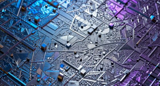
Have you ever wondered how scientists manipulate light at the tiniest scales? It’s fascinating because, at the nanoscale, the rules of classical optics give way to quantum effects, which release a whole new domain of possibilities. Nano-structured films leverage these quantum effects to control light with extraordinary precision. When light interacts with these ultra-thin layers, quantum phenomena like tunneling, interference, and localized surface plasmon resonances come into play. These effects enable devices that can filter, guide, or enhance specific wavelengths of light, making nano-structured films indispensable in modern optics.
Nano-structured films harness quantum effects to precisely control light at the smallest scales.
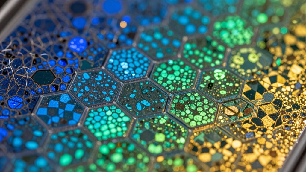
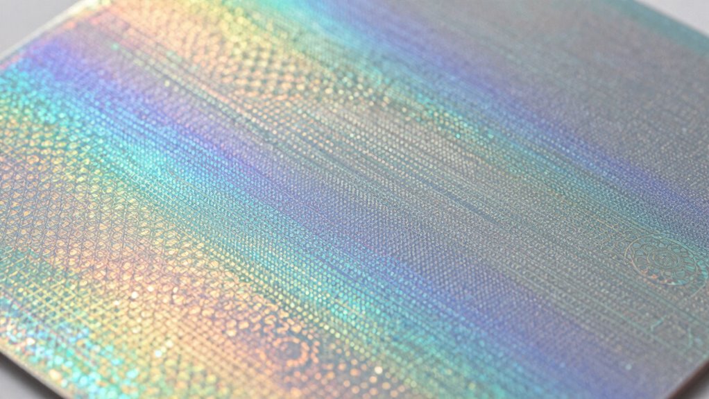
One reason these films are so useful is their ability to undergo surface modifications that tailor their optical properties. By carefully designing the surface features—such as nano-patterns, grooves, or ridges—you can manipulate how light interacts with the film. These surface modifications influence light absorption, reflection, and transmission, allowing for highly customized optical responses. For example, by tweaking the surface topology, you can create anti-reflective coatings that minimize glare or develop highly sensitive sensors that detect minute changes in the environment.
The beauty of nano-structured films lies in their versatility. You can engineer the surface modifications to achieve specific functionalities, whether it’s enhancing light absorption for photovoltaic cells or creating color filters for display technologies. Because the structures are on the nanometer scale, they can resonate at particular wavelengths, amplifying or suppressing certain signals. This capability is a direct result of the quantum effects that dominate at such small dimensions, giving rise to phenomena like surface plasmon resonances that are impossible to achieve with bulk materials. Additionally, the ability to manipulate light at the nanoscale opens up new avenues for developing innovative optical devices.
Moreover, the integration of nano-structured films into optical devices offers significant advantages in miniaturization and performance. Their thinness means they can be incorporated into compact systems without adding bulk, while their tailored surface features ensure high efficiency and specificity. This combination of quantum effects and surface modifications allows for highly sensitive detectors, improved laser components, and advanced imaging systems. As research advances, these films are poised to revolutionize how we manipulate and harness light in everything from telecommunications to biomedical imaging.

Engineering Applications of Polymer based Nano Blends (Advanced Structured Materials, 235)
As an affiliate, we earn on qualifying purchases.
As an affiliate, we earn on qualifying purchases.
Frequently Asked Questions
How Are Nano-Structured Films Manufactured at Large Scale?
You manufacture nano-structured films at large scale by using layer deposition methods like chemical vapor deposition (CVD) or atomic layer deposition (ALD). Then, you apply patterning techniques such as nanoimprint lithography or interference lithography to create precise nanostructures. These processes enable high-throughput production, ensuring uniformity and scalability for industrial applications. By combining layer deposition with advanced patterning, you can efficiently produce complex nano-structured films on a large scale.
What Are the Environmental Impacts of Producing Nano-Structured Films?
Imagine crafting delicate glass sculptures, but with nano-structured films—you’re balancing environmental impacts. Producing these films often involves eco-friendly solvents, reducing harmful emissions, but energy consumption remains high. This energy use is like powering a small city’s worth of lights. While advances aim to lower environmental footprints, you should consider both the benefits of eco-friendly solvents and the ongoing challenge of minimizing energy use, ensuring sustainable innovation in optics.
Can Nano-Structured Films Be Recycled or Reused?
Nano-structured films can be recycled or reused, but recycling challenges exist due to their complex composition and delicate structures. You might find that reuse potential is higher in certain applications, such as coatings or sensors, where the films can be cleaned and repurposed. However, recovering materials from nano-structured films is often difficult, making recycling less straightforward. Advances in sustainable manufacturing could improve their recyclability over time.
How Durable Are Nano-Structured Films Under Extreme Conditions?
You’ll find nano-structured films are remarkably durable under extreme conditions, thanks to their exceptional material resilience and thermal stability. Picture them as tiny, fortified shields that withstand high temperatures, intense radiation, and harsh environments without losing their precision or function. While they’re tough, their durability varies based on composition, but overall, their engineered resilience makes them invaluable for demanding optical applications where stability and longevity are critical.
Are Nano-Structured Films Compatible With Existing Optical Devices?
Yes, nano-structured films are compatible with existing optical devices. They enable seamless optical integration by enhancing device performance without requiring significant modifications. Their material compatibility guarantees they can be integrated with common substrates and components, making them versatile for various applications. You can incorporate these films into your optical systems, benefiting from improved functionalities like better light manipulation, all while maintaining compatibility with current technologies.

Nano Bond Ceramic Coating for Cars – 80% SiO2 Formula, Hydrophobic Paint Protection, UV & Corrosion Resistant for Glass, Wheels & Plastic, Easy Application, Car Detailing Kit, 30ml
Paint Protection That Holds – Your car faces UV rays, salt, acid rain, and scratches every single day….
As an affiliate, we earn on qualifying purchases.
As an affiliate, we earn on qualifying purchases.
Conclusion
You now see how nano-structured films revolutionize modern optics, transforming everyday devices into marvels of technology. Their unique properties, like precise light manipulation and enhanced performance, make them indispensable. Without them, our world would be vastly less brilliant and efficient — almost unimaginable! As you continue exploring, remember these tiny marvels hold the power to shape a future brighter than the sun itself, proving that small things can indeed make the biggest difference.
plasmon resonance filters
As an affiliate, we earn on qualifying purchases.
As an affiliate, we earn on qualifying purchases.

EC Buying 10PCS IR Infrared Sensor Module Slotted Optical Optocoupler Speed Measuring Sensor Module Photo Interrupter Sensor Motor Speed Detection Robot for Arduino
Adopting a slot type photoelectric sensor, it consists of an infrared light-emitting diode and an NPN photoelectric transistor,…
As an affiliate, we earn on qualifying purchases.
As an affiliate, we earn on qualifying purchases.