
Nanoelectronics aims to keep Moore’s Law alive by shrinking transistors to increase performance. But as devices become smaller, quantum tunneling causes leakage currents that waste power and generate heat. This limits how small transistors can get and challenges continued miniaturization. To overcome these hurdles, researchers develop new materials and architectures. If you explore further, you’ll discover how innovations are shaping the future of nanoelectronics amidst quantum effects.
Key Takeaways
- Nanoelectronics enables continued device miniaturization, supporting Moore’s Law by shrinking transistors to nanometer scales.
- Quantum tunneling at nanoscale dimensions introduces leakage currents, challenging the physical limits predicted by Moore’s Law.
- As transistors approach atomic scales, quantum effects threaten to slow or halt the exponential growth in computing power.
- Innovations like high-k dielectrics and FinFET architectures help mitigate tunneling, extending Moore’s Law’s viability.
- Understanding quantum phenomena in nanoelectronics is crucial for developing future transistors that sustain Moore’s Law.
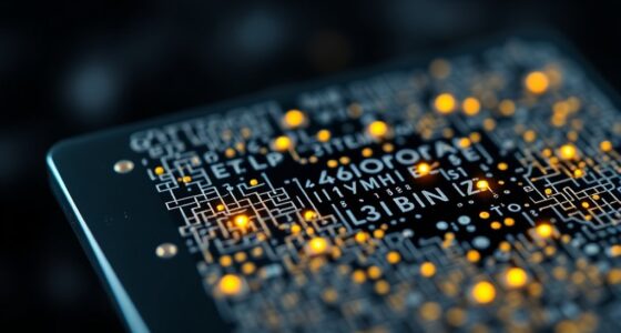
Have you ever wondered how our devices continue to get smaller and more powerful despite the physical limits of traditional electronics? It’s a question that’s driven scientists and engineers to push the boundaries of miniaturization, leading to the fascinating domain of nanoelectronics. At the heart of this progress lies transistor scaling, the process of shrinking transistors to pack more onto a chip. As transistors become smaller, they can switch faster and consume less power, aligning with Moore’s Law’s promise of exponential growth in computing power. But as we push into the nanometer scale, new challenges emerge—most notably, quantum tunneling.
Quantum tunneling occurs when electrons pass through barriers that classical physics would deem impenetrable. In the context of transistor scaling, as the gate oxides and channel regions of transistors shrink to just a few nanometers, electrons can tunnel through these thin barriers, causing leakage currents. These leakage currents become problematic because they waste power and generate heat, undermining the efficiency and reliability of our devices. You might think, “If electrons can tunnel through, doesn’t that mean we’re reaching the physical limits of miniaturization?” It’s a valid concern, and it highlights how quantum effects are no longer negligible at this scale.
Quantum tunneling causes electrons to pass through tiny barriers, leading to leakage currents that challenge transistor miniaturization.
Despite these challenges, researchers are developing innovative solutions to continue transistor scaling. For example, new materials like high-k dielectrics and two-dimensional semiconductors help create better barriers that reduce unwanted tunneling. Additionally, device architectures such as FinFETs and gate-all-around transistors provide improved control over the channel, mitigating leakage caused by quantum tunneling. These advancements allow us to keep shrinking transistors without succumbing to the quantum effects that threaten to stall progress.
In essence, the interplay between transistor scaling and quantum tunneling defines the current frontier of nanoelectronics. You’re witnessing a delicate dance: as we push the physical limits of size, quantum phenomena become more pronounced, demanding inventive engineering solutions. This ongoing innovation not only preserves Moore’s Law but also opens new avenues for ultra-efficient, powerful nanoscale devices. While quantum tunneling presents hurdles, it also offers a deeper understanding of physics at the smallest scales, fueling further breakthroughs. So, even as the laws of classical electronics reach their limits, the quantum sphere invites us to rethink what’s possible, ensuring that the march of technological progress continues well into the future. Moreover, ongoing research into transistor miniaturization aims to find ways to counteract these quantum effects and sustain the pace of technological advancement.

Permatex 22058 Dielectric Tune-Up Grease, 3oz. – High Performance Dielectric Grease Used to Protect Terminals, Spark Plugs, Wiring and Other Electrical Connections Against Salt, Dirt, and Corrosion
Protects Electrical Connections And Wiring From Salt, Dirt And Corrosion
As an affiliate, we earn on qualifying purchases.
As an affiliate, we earn on qualifying purchases.
Frequently Asked Questions
How Does Nanoelectronics Impact Renewable Energy Technologies?
Nanoelectronics boosts renewable energy technologies by enhancing solar efficiency and improving energy storage. You’ll see more efficient solar panels that convert sunlight into electricity more effectively, making renewable energy more accessible. Additionally, nanoelectronics enable better energy storage solutions, allowing you to store excess power for later use. This means more reliable renewable energy systems, reducing reliance on fossil fuels, and helping you contribute to a cleaner, sustainable future.
What Are the Environmental Risks of Nanoelectronics Manufacturing?
You should be aware that manufacturing nanoelectronics can pose environmental risks, mainly due to the production process involving toxic chemicals and manufacturing waste. These substances may contaminate water and soil if not properly managed. Additionally, disposal of nanoelectronics waste could release harmful nanoparticles into the environment. To minimize these risks, strict regulations and eco-friendly practices are essential during manufacturing and disposal processes.
Can Nanoelectronics Enable Quantum Computing Advancements?
Yes, nanoelectronics can enable quantum computing advancements by improving qubit stability and facilitating quantum entanglement. You’ll find that smaller, more precise nanoelectronic components help create more reliable qubits, which are essential for maintaining quantum states. This progress allows for faster, more powerful quantum computers. By enhancing qubit stability and harnessing quantum entanglement, nanoelectronics opens new doors for breakthroughs in quantum technology.
How Do Nanoelectronic Materials Differ From Traditional Semiconductors?
You’ll find nanoelectronic materials totally revolutionize electronics by operating at the molecular scale, unlike traditional semiconductors. They utilize quantum confinement, which drastically alters electrical properties, making devices faster and more efficient. These materials often consist of single molecules or nanostructures, enabling unprecedented control over electron flow. In contrast, traditional semiconductors rely on bulk materials with fixed properties, limiting miniaturization and performance. Nanoelectronics push the boundaries of what’s possible, transforming technology as we recognize it.
What Are the Economic Implications of Reaching Moore’s Law Limits?
Reaching Moore’s Law limits means you’ll see slowed cost reduction in chip manufacturing, which can lead to market saturation as innovation stalls. This could increase device prices, squeeze profit margins, and shift focus toward new technologies like quantum computing or alternative materials. You might also face tougher competition, prompting investments in research and development to find ways around these limits and sustain growth in the tech industry.

FinFET Devices for VLSI Circuits and Systems
As an affiliate, we earn on qualifying purchases.
As an affiliate, we earn on qualifying purchases.
Conclusion
As you see, nanoelectronics push the boundaries of Moore’s Law, enabling smaller, faster, and more efficient devices. But as components shrink further, do you wonder how much longer this trend can continue? The future of technology depends on your innovation and imagination. With each breakthrough, you get closer to unbolting endless possibilities, transforming how we live and work. So, are you ready to be part of this exciting nanoelectronic revolution?

2D Nanoelectronics: Physics and Devices of Atomically Thin Materials (NanoScience and Technology)
As an affiliate, we earn on qualifying purchases.
As an affiliate, we earn on qualifying purchases.

Moore's Law Alive: Gate-All-Around (GAA) Next Generation Transistor
As an affiliate, we earn on qualifying purchases.
As an affiliate, we earn on qualifying purchases.