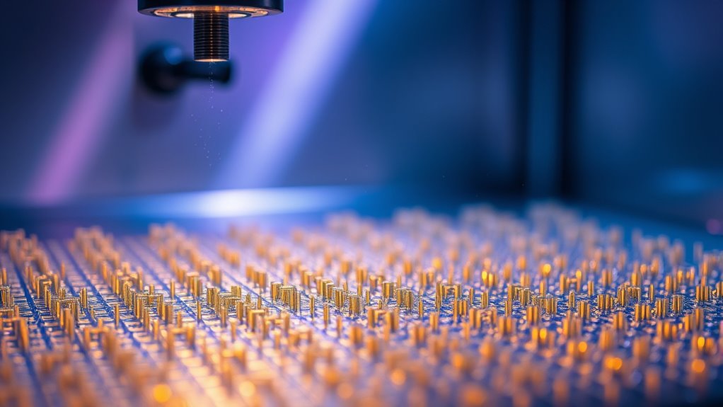

Advanced nanofabrication techniques, like atomic layer deposition (ALD), let you control structures at the atomic level, coating surfaces with precision and creating complex nanodevices. These methods enable you to build high-quality quantum dots, ultra-thin films, and intricate heterostructures with minimal defects. With such tools, you can push the boundaries of nanoelectronics and quantum technologies. If you keep exploring, you’ll discover even more innovative ways to shape the nanoscale world.
Key Takeaways
- Atomic Layer Deposition (ALD) enables atomic-scale, conformal thin film coatings with precise thickness control on complex nanostructures.
- ALD’s self-limiting reactions allow for layer-by-layer fabrication of quantum dots and heterostructures with minimal defects.
- Advanced nanofabrication techniques facilitate precise positioning, size, and composition control of quantum dots for optimized device performance.
- Integration of nanofabrication methods supports the development of complex, multilayered nanoelectronic and photonic devices.
- These techniques push the boundaries of nanoscale engineering, enabling the creation of atomic-scale structures for quantum computing and advanced applications.

Advanced nanofabrication techniques enable scientists and engineers to create structures with atomic-scale precision, opening new possibilities in electronics, medicine, and energy. One of the most exciting developments in this field involves the use of quantum dots—tiny semiconductor particles only a few nanometers in size. These quantum dots exhibit unique optical and electronic properties because of their size-dependent energy levels, making them invaluable for applications like highly efficient solar cells, advanced display technologies, and targeted medical imaging. To precisely position and control these quantum dots, researchers rely on advanced methods such as atomic layer deposition (ALD), a technique that allows for the controlled deposition of thin films one atomic layer at a time. ALD’s ability to produce uniform, conformal coatings on complex nanostructures ensures that quantum dots are integrated seamlessly into devices with minimal defects or inconsistencies.
Using atomic layer deposition, you can achieve exceptional precision, layering materials with atomic-scale accuracy. This process involves exposing a substrate to alternating precursor gases that react with the surface in a self-limiting manner. As a result, each cycle deposits a single atomic layer, enabling you to build multilayered structures with unparalleled control. When combined with quantum dot fabrication, ALD allows you to tailor the size, composition, and placement of quantum dots, optimizing their properties for specific applications. For example, in optoelectronics, you can fine-tune the bandgap of quantum dots by controlling their size, which directly impacts their light absorption and emission characteristics. This level of control guarantees you can design devices with enhanced performance and efficiency. Additionally, these methods support the fabrication of atomic-scale structures, which are crucial for advancing nanoelectronics and quantum technologies.
Moreover, advanced nanofabrication techniques like atomic layer deposition support the development of complex heterostructures, where different materials are layered with atomic precision. This capability is essential for creating quantum dot-based devices that require precise interfaces and minimal defect densities. As you work with these methods, you’ll find that they also enable the integration of quantum dots into flexible substrates or three-dimensional architectures, broadening their potential applications. The synergy between quantum dot technology and atomic layer deposition is transforming fields such as quantum computing, photonics, and biomedicine—pushing the boundaries of what you can achieve at the nanoscale. With these techniques, you’re not just building tiny structures; you’re shaping the future of advanced technology with atomic-level accuracy and control.

Handbook of Thin Film Deposition
As an affiliate, we earn on qualifying purchases.
As an affiliate, we earn on qualifying purchases.
Frequently Asked Questions
What Are the Environmental Impacts of Nanofabrication Processes?
You should be aware that nanofabrication processes can impact the environment through waste generation and chemical use. Proper waste management is essential to prevent pollution, while adherence to environmental regulation helps minimize risks. By following best practices, you can reduce hazardous emissions and guarantee safer disposal of nanomaterials, ultimately protecting ecosystems and public health. Staying informed and compliant makes your nanofabrication efforts more sustainable and environmentally responsible.
How Do Nanofabrication Techniques Vary Across Different Industries?
You’ll find nanofabrication techniques vary across industries through industry-specific applications and process customization. In electronics, you use precise lithography for miniaturized chips, while in healthcare, you tailor processes to create nanocarriers for drug delivery. Manufacturing adapts techniques to suit material demands, and energy sectors focus on optimizing nanoscale catalysts. By customizing the process, industries achieve unique functionalities, making nanofabrication versatile across various fields.
What Are the Ethical Considerations in Nanotechnology Development?
You need to contemplate ethical issues like genetic privacy and human enhancement when developing nanotechnology. As you innovate, guarantee you protect personal genetic data from misuse, and think about how your work could enhance human abilities ethically. Balancing technological progress with societal values is vital to prevent potential misuse or harm. By addressing these concerns proactively, you help promote responsible development that benefits society while respecting individual rights.
How Cost-Effective Are Advanced Nanofabrication Methods?
You’ll find advanced nanofabrication methods can be quite cost-effective, often reducing manufacturing costs by up to 30%. This boosts cost efficiency because these techniques allow for precise, high-volume production with minimal material waste. While initial setup can be expensive, the long-term savings and improved quality make them a smart investment. Over time, you’ll see these methods help lower overall costs and accelerate product development.
What Are the Future Trends in Nanofabrication Research?
You should expect future nanofabrication research to focus on quantum lithography and 3D nanoprinting. These trends aim to push the limits of resolution, enabling you to create incredibly precise and complex nanoscale structures. As technology advances, you’ll see more integration of quantum effects for better patterning and innovative 3D printing techniques, making nanofabrication faster, more versatile, and accessible for applications across electronics, medicine, and materials science.
Quantum dot fabrication kit
As an affiliate, we earn on qualifying purchases.
As an affiliate, we earn on qualifying purchases.
Conclusion
By mastering advanced nanofabrication techniques, you push the boundaries of what’s possible at the smallest scales. Some believe these methods could revolutionize industries, while others argue challenges like scalability and precision remain. As you explore this field, remember that ongoing research continues to test these theories. Your work could help confirm or challenge these ideas, shaping future innovations in nanotechnology. Embrace the complexity—you’re on the frontier of transforming science and technology.

Kaisiking 6 Pcs Double Sided Soldering Assist Aid Repair Tool with 2 Precision Tweezers for Electronics Repair and Soldering
Soldering tools kit includes 6 double-sided soldering assist tool and 2 precision Tweezers, More flexible and convenient when…
As an affiliate, we earn on qualifying purchases.
As an affiliate, we earn on qualifying purchases.

100% FILM for SVS System Incl. 6 Rolls (Fits Accuri & Strata 1 Adult)
Replacement 6 pack of films for the SVS system
As an affiliate, we earn on qualifying purchases.
As an affiliate, we earn on qualifying purchases.