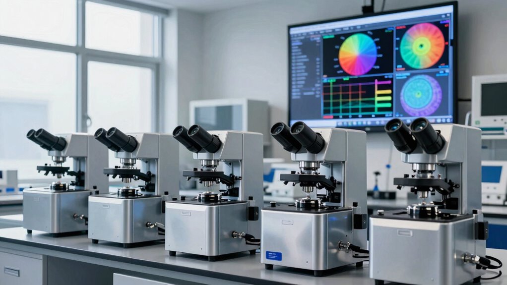

In 2026, I’ve come across four top AFMs that really stand out for surface analysis. They enhance measurement accuracy through advanced detection systems and are designed for compatibility with polished silicon wafer substrates. Plus, they offer robust environmental controls to maintain stability during imaging. Each AFM’s unique features cater to specific research needs, ensuring high-quality data collection. Stay tuned, and I’ll share more insights about these exceptional tools and their applications in your research.
Key Takeaways
- Look for AFMs with advanced detection systems for high-resolution imaging, essential for distinguishing nanometer-scale features in surface analysis.
- Ensure the AFM systems offer environmental control features to maintain stability and prevent contamination during measurements.
- Choose models compatible with various substrates, like polished silicon wafers, for consistent and reliable results across different research applications.
- Opt for AFMs that provide thorough user training and technical support to enhance operation efficiency and data interpretation accuracy.
- Prioritize systems that incorporate active monitoring and feedback mechanisms to ensure optimal performance and long-term reliability in surface analysis.
| Surface Analysis with STM and AFM Techniques | 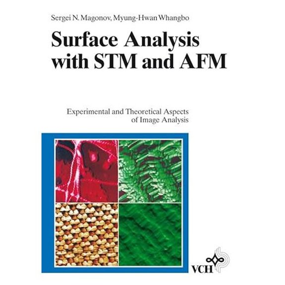 | Comprehensive Reference | Material: Not specified | Surface Finish: Not specified | Package Quantity: Not specified | VIEW LATEST PRICE | See Our Full Breakdown |
| Polished Silicon Wafer Substrate for Laboratory Research |  | Precision Performance | Material: High-purity single crystal silicon | Surface Finish: Mirror-smooth surface with low roughness | Package Quantity: 10 pieces per bag | VIEW LATEST PRICE | See Our Full Breakdown |
| Polished Silicon Wafer Substrate for Laboratory Research | | Versatile Research Tool | Material: High-purity single crystal silicon | Surface Finish: Mirror-smooth surface with low roughness | Package Quantity: 10 pieces per bag | VIEW LATEST PRICE | See Our Full Breakdown |
| Polished Silicon Wafer Substrate for Laboratory Research | | Compact Laboratory Essential | Material: High-purity single crystal silicon | Surface Finish: Mirror-smooth surface with low roughness | Package Quantity: 10 pieces per bag | VIEW LATEST PRICE | See Our Full Breakdown |

More Details on Our Top Picks
-
B0G1BW6KCF
Amazon Product B0G1BW6KCF
As an affiliate, we earn on qualifying purchases.
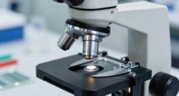
Surface Analysis with STM and AFM Techniques
When it comes to exploring surface structures at the atomic level, “4 Top AFMs for Surface Analysis in 2026” is perfect for researchers and newcomers alike who want to deepen their understanding of STM and AFM techniques. These powerful tools allow us to examine surfaces at atomic and molecular scales, revealing essential topographical and electronic information. However, many past studies faced challenges due to inadequate theoretical understanding. I’ve found that grasping how measurement conditions influence image patterns is indispensable. By simulating images and understanding tip-sample interactions, we can better distinguish true surface features from artifacts, enhancing our research’s accuracy and reliability.
- Material:Not specified
- Surface Finish:Not specified
- Package Quantity:Not specified
- Application:STM and AFM surface analysis
- Size:Not specified
- Research Use:Suitable for researchers in STM and AFM
- Additional Feature:Comprehensive theoretical analysis
- Additional Feature:Image simulation techniques
- Additional Feature:Focus on inorganic materials
-
B0G1BVB6P5
Amazon Product B0G1BVB6P5
As an affiliate, we earn on qualifying purchases.
Polished Silicon Wafer Substrate for Laboratory Research
For researchers seeking high-quality substrates for advanced surface analysis, the polished silicon wafer substrate stands out as an ideal choice. I’ve found these wafers perfect for SEM and AFM analysis, thanks to their mirror-smooth surface and low roughness. Each 3x3mm wafer is crafted from high-purity single crystal silicon, ensuring stability and consistent measurement results. They come in packs of ten, making handling and alignment straightforward. Whether you’re working on thin film deposition or semiconductor research, these wafers deliver reliable performance across various analytical techniques, supporting your advanced research and development efforts efficiently.
- Material:High-purity single crystal silicon
- Surface Finish:Mirror-smooth surface with low roughness
- Package Quantity:10 pieces per bag
- Application:SEM and AFM analysis
- Size:3x3mm
- Research Use:Suitable for laboratory research
- Additional Feature:Mirror-smooth surface quality
- Additional Feature:High-purity single crystal
- Additional Feature:Easy handling design
-
B0G1BR57LX
Amazon Product B0G1BR57LX
As an affiliate, we earn on qualifying purchases.
Polished Silicon Wafer Substrate for Laboratory Research
Researchers focused on surface analysis will find that polished silicon wafer substrates are indispensable for their work. These high-purity, single crystal silicon substrates are designed for stability and consistent performance, making them ideal for microanalysis and semiconductor research. With a mirror-smooth surface and low roughness, they’re perfect for SEM and AFM analysis. I love the square cut design, which allows for easy mounting and precise alignment. Available in standard sizes like 40x40mm, they come in packages of ten, ensuring I always have enough for my laboratory needs. These substrates truly enhance measurement and coating performance in any research environment.
- Material:High-purity single crystal silicon
- Surface Finish:Mirror-smooth surface with low roughness
- Package Quantity:10 pieces per bag
- Application:SEM and AFM analysis
- Size:40x40mm
- Research Use:Suitable for laboratory research
- Additional Feature:Standard size: 40x40mm
- Additional Feature:Double-side polished option
- Additional Feature:Reliable measurement performance
Polished Silicon Wafer Substrate for Laboratory Research
Polished silicon wafer substrates are essential for anyone delving into advanced laboratory research, especially in the domain of microanalysis and semiconductor studies. These high-purity, single crystal silicon wafers provide a stable, flat surface, ensuring precise measurements. With a mirror-smooth finish and low roughness, they’re perfect for applications like SEM and AFM. Each square-cut wafer, typically 10x10mm, is processed for easy mounting and alignment, making them ideal for surface morphology testing and thin film deposition. Supplied in packs of ten, each piece meets super polish standards, catering to the rigorous demands of material analysis in research labs.
- Material:High-purity single crystal silicon
- Surface Finish:Mirror-smooth surface with low roughness
- Package Quantity:10 pieces per bag
- Application:SEM and AFM analysis
- Size:10x10mm
- Research Use:Suitable for laboratory research
- Additional Feature:Super polish standards
- Additional Feature:Designed for microanalysis
- Additional Feature:Precise flat square forms
Factors to Consider When Choosing AFM for Surface Analysis

When choosing an AFM for surface analysis, I think about several key factors that can really impact the results. Resolution and imaging capability are vital, but I also consider sample compatibility and the accuracy of surface roughness measurements. Additionally, I can’t overlook the importance of tip selection, maintenance, and the software used for data analysis.
Resolution and Imaging Capability
Choosing the right AFM for surface analysis hinges considerably on its resolution and imaging capabilities. The resolution determines your ability to distinguish features at the nanometer or even sub-nanometer scale, which directly affects the clarity of surface details. Higher resolution AFMs typically utilize sharper tips and advanced detection systems, allowing for precise imaging of topography. Additionally, the imaging capability includes both topographical and mechanical property measurements, relying on the instrument’s sensitivity and tip quality. When selecting an AFM, I recommend considering its maximum achievable resolution relative to the size of the surface features you’re interested in. Keep in mind that factors like tip wear, vibration noise, and environmental conditions can also influence resolution and ultimately degrade image quality.
Sample Compatibility Requirements
Understanding sample compatibility is essential for successful surface analysis with an AFM. I always ensure the AFM I choose matches the sample’s size, shape, and material to avoid any damage and achieve accurate results. It’s vital to verify that the AFM’s scan mode and tip type align with the surface properties and resolution needs of the sample. I also check that the sample’s surface chemistry won’t adversely interact with the AFM tip or lead to contamination during analysis. Additionally, I assess the AFM’s ability to accommodate the sample’s environmental needs, whether in vacuum, liquid, or controlled atmosphere. Finally, I consider the sample’s stability and fragility to select an AFM setup that minimizes potential surface alterations during scanning.
Surface Roughness Measurement Accuracy
Achieving accurate surface roughness measurements with an AFM hinges on several critical factors that I consider carefully. First, I ensure I select a probe with an appropriate tip radius; smaller tips deliver higher resolution for capturing fine features. Next, I rely on calibration standards with known roughness values to validate my measurements. The imaging mode I choose—whether contact, tapping, or non-contact—also plays a significant role, as each interacts differently with the surface topography. I make it a priority to maintain minimal tip wear and contamination, as degradation can skew results. Finally, I pay close attention to scan size and resolution settings, opting for higher resolution scans over smaller areas to achieve precise roughness data.
Tip Selection and Maintenance
When selecting an AFM tip, it’s vital to take into account the specific requirements of your surface analysis, as the right choice can greatly influence your results. The material of the tip, whether silicon or diamond, affects resolution and durability, so consider your surface type carefully. Tip sharpness, often in the nanometer range, is key for accurately resolving atomic-scale features. Regularly cleaning and calibrating the tip helps maintain imaging quality and avoid contamination. Additionally, different geometries, like pyramidal or spherical, can impact interaction forces and interpretation of surface features. If you’re focused on specific imaging modes, coating tips with conductive or specialized materials can markedly enhance performance. Make these considerations a priority for ideal results.
Software and Data Analysis
Selecting the right software for your AFM is essential since it can profoundly impact the quality of your surface analysis. I always look for software that offers real-time image processing, noise reduction, and advanced filtering options to enhance data interpretation. Ensuring compatibility with various data formats like TIFF and ASCII is also important for seamless integration into my analysis workflows. Analytical features such as surface roughness calculation and 3D rendering help me quantify surface characteristics accurately. A user-friendly interface and customizable measurement protocols boost my efficiency and reproducibility in tasks. Finally, robust data management and export capabilities make documenting, sharing, and further analyzing AFM results a breeze, making my research process smoother and more productive.
Environmental Control Features
Environmental control features are essential for ensuring accurate and reliable surface analysis with AFM. I always consider temperature and humidity regulation because they minimize surface contamination and drift during imaging. An enclosed or vibration-isolated AFM system is vital for reducing external disturbances that can affect measurement accuracy, particularly in sensitive analyses. Controlled atmospheres, such as inert gas environments or vacuum chambers, help prevent oxidation and contamination, ensuring the data’s integrity. I find that precise environmental regulation markedly enhances reproducibility and allows for high-resolution imaging of delicate surfaces. Additionally, advanced AFM instruments often come with active environmental monitoring and feedback systems, which maintain ideal conditions throughout the measurement process, making my analysis more dependable and effective.
User Training and Support
While choosing an AFM for surface analysis, I can’t emphasize enough the importance of user training and support. Adequate training ensures I operate the AFM precisely, minimizing measurement errors and misinterpretations. Understanding tip-sample interactions is vital for obtaining accurate surface topography and property data. Extensive support from manufacturers or technical teams is invaluable when troubleshooting complex imaging or calibration issues. Ongoing assistance, like software tutorials and maintenance guidance, helps guarantee ideal AFM performance over time. When I’m well-trained, I’m better equipped to interpret AFM data correctly, avoiding common pitfalls related to artifacts. So, always consider the quality of training and support when selecting an AFM; it can markedly impact your analysis outcomes.
Frequently Asked Questions
How Do AFMS Compare to Other Surface Analysis Techniques?
AFMs offer unique advantages over other surface analysis techniques. I’ve found they provide high-resolution imaging and can measure surface topography at the nanoscale, which many methods can’t achieve. While techniques like SEM or XPS are great for elemental analysis, AFMs excel in studying surface forces and mechanical properties. I’ve often relied on AFMs for detailed insights, making them invaluable for my research, especially when precision and surface detail are essential.
What Are the Costs Associated With Purchasing an AFM?
Purchasing an AFM can range from $100,000 to over $500,000, depending on the model and features. I’ve found that additional costs, like maintenance, accessories, and software, can add considerably to the price. If you’re considering one, it’s crucial to factor in these expenses to get a full picture. I recommend researching various models and speaking to vendors to find the best fit for your budget and requirements.
Can AFMS Analyze Biological Samples Effectively?
Absolutely, AFMs can analyze biological samples effectively! I’ve seen their precision in visualizing cellular structures and even proteins. With their ability to operate in liquid environments, they’re perfect for studying live cells. I’ve marveled at how they reveal details at the nanoscale, which traditional techniques often miss. It’s fascinating how AFMs bridge the gap between biology and nanotechnology, allowing us to explore the microscopic world in ways we never thought possible.
How Often Should AFMS Be Calibrated for Accurate Results?
I usually calibrate my AFM every few months to guarantee accurate results, but it really depends on how frequently I use it and the specific applications. If I’m working with delicate biological samples or in a high-precision environment, I might check calibration more often. Regular maintenance and calibration help me maintain consistency in my measurements, which is vital for reliable data. Always trust your instincts and adjust based on your specific needs!
What Is the Average Lifespan of an AFM Instrument?
The average lifespan of an AFM instrument typically ranges from 5 to 10 years, depending on usage and maintenance. I’ve found that regular servicing and proper care can extend its life considerably. It’s essential to monitor performance and address any issues promptly. In my experience, investing in quality components and following manufacturer guidelines pays off. This way, I guarantee the AFM remains dependable and delivers precise results throughout its lifespan.
Conclusion
In conclusion, as we look to the horizon of surface analysis in 2026, embracing the advancements in AFM technology will undoubtedly elevate our research endeavors. While the polished silicon wafer substrate serves as a reliable canvas, the factors we’ve discussed will guide us toward the ideal AFM instrument. By thoughtfully steering these choices, we can unlock new dimensions in our work, allowing us to indulge in the subtle nuances of surface characterization with elegance and precision.