
Beyond graphene, many new 2D materials like transition metal dichalcogenides, hexagonal boron nitride, black phosphorus, and MXenes are emerging with unique features such as tunable bandgaps, high mobility, and excellent conductivity. While big challenges remain in scaling up production, researchers are developing innovative synthesis methods and device applications that harness these materials’ properties. Keep exploring to discover how these advances are shaping the future of electronics, energy, and beyond.
Key Takeaways
- Diverse 2D materials like TMDs, h-BN, black phosphorus, MXenes, and Xenes offer unique electronic, optical, and catalytic properties beyond graphene.
- Scalable synthesis methods such as CVD and exfoliation are advancing to enable large-area, high-quality production of new 2D materials.
- Novel device applications include high-performance transistors, photodetectors, and energy storage systems utilizing these emerging 2D layers.
- Property engineering through doping, heterostructures, and strain tuning enhances functionality and customizes material behavior.
- Future trends focus on heterostructure innovation, AI-driven discovery, and overcoming stability and scalability challenges for commercial use.

224 PCS STEM Building Toys for Kids Ages 4-8, Creative Mosaic Drill Set with Electric Drill & Screwdriver, 2D/3D Building Blocks Kit, Educational Birthday Gift for 5 6 7 8 9 10 Year Old Boys Girls
【ULTIMATE STEM LEARNING KIT】 Inspire your little engineer’s imagination! This 224-piece STEM building set focuses on enhancing science,…
As an affiliate, we earn on qualifying purchases.
As an affiliate, we earn on qualifying purchases.
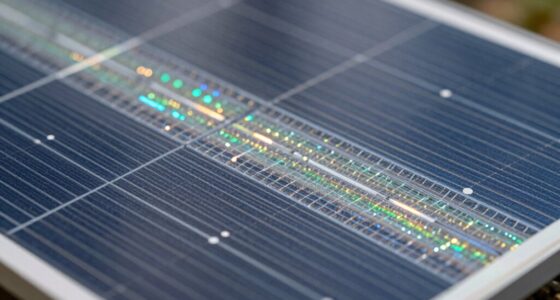
Exploring Alternative 2D Materials and Their Unique Features
While graphene dominates 2D material research, exploring alternatives reveals a range of unique features suited for specific applications. You discover transition metal dichalcogenides (TMDs) with tunable bandgaps and high carrier mobility, ideal for semiconductors. Hexagonal boron nitride (h-BN) offers excellent insulating properties, making it perfect as a dielectric layer. Black phosphorus (BP) or phosphorene provides a direct bandgap and anisotropic charge transport, useful in optoelectronics. MXenes, with their metallic conductivity and high surface reactivity, excel in catalytic and energy storage applications. Xenes like silicene and germanene, with their graphene-like lattices, show promise for flexible electronics. Exploring these materials allows you to tailor properties for specific device needs, overcoming graphene’s limitations and broadening 2D material applications. Additionally, understanding the synthesis techniques for these materials is crucial for advancing their practical use.

Graphene from Natural Sources: Synthesis, Characterization, and Applications
As an affiliate, we earn on qualifying purchases.
As an affiliate, we earn on qualifying purchases.
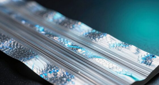
Overcoming Synthesis Challenges for Scalable Production

Scaling up the production of 2D materials remains a significant hurdle due to their complex multi-element layered structures, which are more challenging to synthesize than single-element graphene. To overcome this, you should focus on key strategies:
Scaling 2D materials production requires advanced synthesis, exfoliation, and process control for quality and scalability.
- Improving chemical vapor deposition (CVD) techniques for uniform, large-area films.
- Developing scalable exfoliation methods that maintain high quality.
- Employing electrochemical engineering to produce defect-controlled layers.
- Enhancing process control for consistency and reproducibility in mass production.
- Incorporating real-time monitoring techniques to ensure process stability and quality assurance.
- Advancing fabrication innovations to develop more efficient and reliable synthesis methods.
- Implementing process automation to optimize throughput and reduce variability in large-scale manufacturing.
Furthermore, integrating quality assurance protocols throughout the production process can significantly improve yield and material consistency. Additionally, adopting standardized testing methods can help in maintaining uniformity across different batches. These approaches aim to address scalability and quality issues, enabling broader application. Overcoming synthesis challenges requires innovation in fabrication methods and precise process control. This progress is crucial to access the full potential of diverse 2D materials beyond graphene.

OWOFYDR 2N2222/2N2222A NPN General Purpose Transistor, 100Pcs TO-92 for High-Frequency Amplifier, High-Speed Switching, Relay Drive & LED Switch Circuits
PRECISION DUAL-MODE PARAMETERS – This pack includes the 2N2222A (40V VCEO, 0.8A IC) version. It features 250MHz transition…
As an affiliate, we earn on qualifying purchases.
As an affiliate, we earn on qualifying purchases.
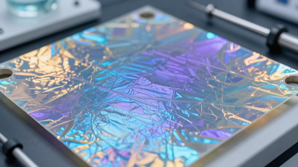
Device Innovations Leveraging New 2D Materials

Advancements in synthesis methods have paved the way for innovative device designs that harness the unique properties of emerging 2D materials. You can now develop high-performance field-effect transistors using transition metal dichalcogenides (TMDs) and black phosphorus, thanks to their tunable bandgaps and high carrier mobilities. Photodetectors benefit from the strong light absorption and direct bandgaps of these materials, enabling sensitive optical sensing in the visible and near-infrared ranges. Heterostructures combine different 2D layers to create flexible, transparent electronics, while supercapacitors and solar cells use MXenes’ metallic conductivity and high surface reactivity for enhanced energy storage. Additionally, the synthesis techniques employed to produce these materials continue to improve, allowing for scalable and cost-effective manufacturing. The development of scalable fabrication methods supports the transition from research to commercial applications. By integrating these materials, you can push the boundaries of device performance, adaptability, and miniaturization, opening new avenues in electronics, optoelectronics, and energy technologies.

2D Materials for Energy Storage and Conversion
As an affiliate, we earn on qualifying purchases.
As an affiliate, we earn on qualifying purchases.
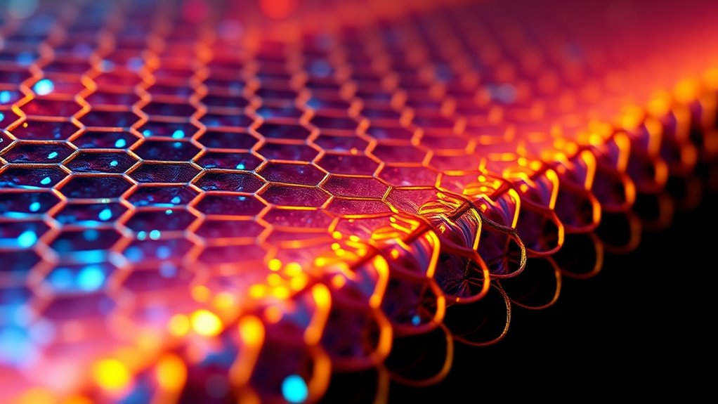
Engineering Strategies to Tailor Material Properties

Engineering strategies play a crucial role in customizing the properties of 2D materials to meet specific device requirements. You can modify these materials through various methods:
- Doping: Introducing foreign atoms alters electronic properties, enabling bandgap tuning and conductivity control.
- Heterostructure Formation: Stacking different 2D layers creates interfaces with unique optoelectronic behaviors.
- Strain Engineering: Applying mechanical strain adjusts lattice parameters, influencing electronic and optical characteristics.
- Defect Engineering: Creating or healing defects modifies surface reactivity and charge transport pathways.
- Natural Composition and Structure: Understanding the natural composition and structure of 2D materials helps tailor their properties effectively.
These approaches allow you to optimize materials for applications like transistors, sensors, and energy devices. Combining techniques offers precise control over properties, pushing the boundaries of what 2D materials can achieve beyond their inherent limitations.
Future Perspectives in 2D Material Research and Applications

Future research in 2D materials is poised to transform their practical applications by focusing on innovative strategies that overcome current limitations. You’ll see advancements in heterostructure engineering, where stacking different 2D layers creates new functionalities. Doping control and defect engineering will fine-tune electronic and optical properties, expanding device possibilities. AI-assisted discovery accelerates identifying promising materials with tailored features. Strain and moiré pattern engineering will release novel phenomena like exotic magnetism and tunable photonics. Overcoming stability issues and improving large-scale synthesis are key to commercialization. As you explore these developments, expect more robust, versatile materials that meet specific demands in electronics, energy, and sensing. These efforts will drive 2D materials beyond research labs into real-world applications, shaping future technologies. Emerging synthesis techniques will be crucial for scaling up production and ensuring material stability.
Frequently Asked Questions
What Are the Environmental Impacts of Large-Scale 2D Material Synthesis?
You should consider that large-scale 2D material synthesis can impact the environment through energy consumption, chemical waste, and resource depletion. Manufacturing processes often involve hazardous chemicals, which may lead to pollution if not properly managed. Additionally, high energy use contributes to carbon emissions. To minimize these impacts, you can focus on greener synthesis methods, recycle chemicals, and optimize processes for sustainability, helping protect the environment while advancing 2D materials.
How Do 2D Materials Compare Cost-Wise to Traditional Semiconductors?
You’ll find that 2D materials can be more expensive than traditional semiconductors due to complex synthesis methods like chemical vapor deposition and exfoliation, which often require costly equipment and processes. However, as production techniques improve and scale up, costs are expected to decrease. While initial expenses are higher, their unique tunable properties and potential for advanced applications may justify the investment, especially in high-performance or specialized devices.
Are There Biocompatible 2D Materials Suitable for Medical Applications?
Yes, there are biocompatible 2D materials suitable for medical applications. You might consider materials like black phosphorus, which shows promise due to its biodegradability and good charge mobility, or hexagonal boron nitride, known for its inertness and safety. These materials can be integrated into biosensors, drug delivery systems, and tissue engineering, offering potential in biocompatible device development. Their safety profiles make them attractive for various medical uses.
What Are the Long-Term Stability Considerations for 2D Heterostructures?
You should consider that long-term stability of 2D heterostructures depends on factors like environmental exposure, material interactions, and structural integrity. You need to guarantee proper encapsulation to prevent degradation from moisture, oxygen, and temperature changes. Doping and defect control can also improve stability. Regular testing and protective coatings help maintain performance over time, making these structures viable for practical applications.
How Can AI Accelerate Discovery of New 2D Materials?
AI accelerates discovery of new 2D materials by analyzing vast datasets to identify promising candidates quickly. For example, a case study shows AI predicting novel TMDs with optimized bandgaps for electronics. You can use machine learning algorithms to model how different synthesis conditions affect material properties, streamlining experimentation. This approach reduces trial-and-error, speeds up material discovery, and helps you develop innovative 2D materials tailored to specific applications faster than traditional methods.
Conclusion
As you explore the vibrant landscape beyond graphene, imagine revealing a palette of 2D materials, each with unique colors and textures waiting to transform your innovations. Overcoming synthesis hurdles feels like opening secret doors to scalable production, opening endless possibilities. With device breakthroughs and clever engineering, you can shape a future where these atomic layers weave into smarter, more powerful technologies. The horizon sparkles with promise—your journey into 2D materials is just beginning.