
Your nano-scale structure directly affects how electrons move, influencing conductivity. Smaller sizes and shapes create surface effects and energy states that can enhance or hinder electron flow through quantum tunneling and confinement. Atomic arrangements and defects also play a role, with well-ordered structures promoting higher strength and better conduction while irregularities cause barriers. Interfaces between materials further modify these properties, offering precise control over performance. Keep exploring to understand how these factors come together to shape electrical behavior and material strength.
Key Takeaways
- Nano-structure size and shape directly affect electron confinement, mobility, and quantum tunneling, altering electrical conductivity.
- Atomic arrangement and defect levels influence electron pathways, impacting both conductivity and material strength.
- Interfaces between nano-materials create potential barriers or wells, modifying electron flow and tunneling effects.
- Surface effects become prominent at nano-scale, introducing energy states that can enhance or hinder electrical conduction.
- Structural design at the nano-level determines the balance between electrical performance and mechanical strength.

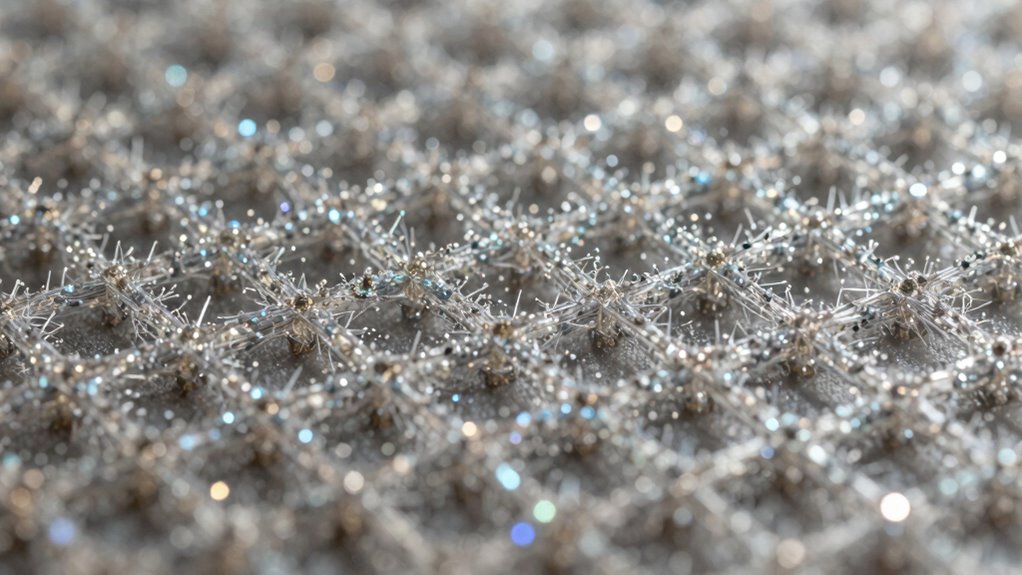
Have you ever wondered how materials at the nano-scale can profoundly alter their electrical properties? When structures shrink to such tiny dimensions, their behavior changes in ways that are both fascinating and useful. At the nano-scale, electrons don’t follow the same rules they do in bulk materials. Instead, quantum effects become notable, particularly phenomena like quantum tunneling, which allows electrons to pass through barriers they normally couldn’t overcome. This process can either increase or decrease electrical conductivity, depending on how the nano-structure is designed. For example, in ultra-thin layers or nanowires, electrons can tunnel across gaps or barriers, effectively creating new pathways for electrical flow. As a result, the overall electron mobility—the ease with which electrons move through a material—can be profoundly affected. Higher electron mobility generally means better conductivity, but at the nano-scale, this relationship becomes more complex due to quantum tunneling. If the nano-structures are engineered to facilitate tunneling, you might see an increase in conductivity, even in materials that would otherwise be poor conductors. Conversely, if barriers are intentionally introduced or become unavoidable due to size effects, tunneling can hinder electron flow, reducing conductivity.
The size and shape of these nano-structures directly influence how electrons behave. When you shrink materials down to the nano-scale, surface effects become dominant because a larger proportion of atoms are on the surface. This can introduce new energy states that modify electron mobility, either enhancing or impeding electrical conduction. The arrangement of atoms and the presence of defects at this scale also play a vital role. For instance, a well-ordered nano-structure with minimal defects allows electrons to move more freely, boosting conductivity. On the other hand, irregularities and grain boundaries can act as barriers, trapping electrons and decreasing mobility. Additionally, the interface between different nano-materials can create potential barriers or wells, which influence quantum tunneling and electron flow. By manipulating these interfaces, you can engineer materials with tailored electrical properties suited for specific applications. Moreover, the cultural significance of indigenous practices often emphasizes harmony with natural materials, which can inspire sustainable approaches in nano-engineering and material design. Understanding the interplay between quantum mechanics and atomic arrangements**** is crucial for advancing nano-electronic technologies, as it helps in predicting and controlling material behavior at these scales.
In essence, nano-scale structures influence conductivity and strength through a delicate interplay of quantum mechanics and atomic arrangements. Quantum tunneling at these scales allows electrons to bypass traditional barriers, substantially altering electron mobility. How you design and control these tiny features determines whether a material becomes a highly conductive nanowire or a more resistive film. Understanding these principles enables you to develop advanced materials with customized electrical behaviors, paving the way for innovations in electronics, sensors, and energy storage.

Conductive Silicone, Highly Electrical Conductive Paint Designed Using Nanotechnology, Strong Adhesion, Waterproof, Flexible, Perfect for Repairing Rubber Buttons in Remote Controls & keypads (1oz)
Multipurpose Conductive silicone : Use it for everything from simple electric repairs like rubber keypad buttons to complex…
As an affiliate, we earn on qualifying purchases.
As an affiliate, we earn on qualifying purchases.
Frequently Asked Questions
How Does Temperature Affect Nano-Scale Structural Properties?
You’ll find that temperature impacts nano-scale structures profoundly. As temperature rises, thermal expansion causes atoms to vibrate more, which can weaken structural integrity. It also influences quantum tunneling by altering electron pathways, potentially changing conductivity. Conversely, lower temperatures reduce atomic vibrations, maintaining strength and allowing more predictable quantum tunneling. So, managing temperature is essential to optimize both conductivity and strength in nano-scale materials.
Can Nano-Structures Improve Material Durability Over Traditional Designs?
Imagine a car’s body made with nano-structured materials, which considerably boosts durability. Nano structure durability enhances material resilience by preventing cracks and wear over time, outperforming traditional designs. This innovation leads to longer-lasting, lightweight, and stronger products. By integrating nano-scale structures, you can revolutionize material innovation, making everyday objects more durable and reliable, ultimately transforming industries like automotive, aerospace, and electronics with smarter, more resilient materials.
What Manufacturing Challenges Exist for Nano-Scale Structures?
You face manufacturing challenges like controlling surface roughness at the nano-scale, which affects the uniformity and performance of nano-structures. Precise fabrication methods are necessary to prevent defects that could cause quantum tunneling, leading to unintended conductivity issues. Achieving consistent, defect-free structures requires advanced techniques, often increasing complexity and cost. Overcoming these hurdles is essential for harnessing the full potential of nano-scale materials in applications demanding high conductivity and strength.
How Do Defects at the Nano-Scale Impact Conductivity?
Imagine tiny defects as roadblocks on a busy highway, slowing down electrons. These imperfections cause increased electron scattering, reducing conductivity. In some cases, defects enable quantum tunneling, letting electrons pass through barriers they normally wouldn’t, which can either enhance or disrupt conductivity. You might think of it like a shortcut—sometimes helpful, sometimes causing traffic jams. Overall, nano-scale defects markedly influence electrical performance by altering electron flow.
Are Nano-Structures Scalable for Industrial Applications?
Nano-structures are scalable for industrial applications when you utilize advanced nano assembly techniques and surface modification strategies. These methods allow you to precisely create and manipulate nanoscale features, ensuring consistent quality and performance. By optimizing fabrication processes and surface properties, you can integrate nano-structures into larger systems effectively, making them suitable for electronics, materials, and other industries. This scalability hinges on your ability to control and reproduce nano-scale features reliably.
nano-structured strength testing equipment
As an affiliate, we earn on qualifying purchases.
As an affiliate, we earn on qualifying purchases.
Conclusion
In the world of nanostructures, tiny changes can have big impacts on conductivity and strength. You see, by controlling the nano-scale, you reveal new possibilities for smarter, stronger materials. Remember, “a chain is only as strong as its weakest link” — so, by mastering nano-structures, you reinforce the very foundation of future innovations. Embrace these small-scale tweaks, and you’ll pave the way for breakthroughs that could reshape technology as we understand it.

NONEQUILIBRIUM QUANTUM TRANSPORT PHYSICS IN NANOSYSTEMS: FOUNDATION OF COMPUTATIONAL NONEQUILIBRIUM PHYSICS IN NANOSCIENCE AND NANOTECHNOLOGY
As an affiliate, we earn on qualifying purchases.
As an affiliate, we earn on qualifying purchases.
The Nano-Pico Interface: Precision Engineering for Next-Generation Materials (Lecture Notes in Nanoscale Science and Technology, 52)
As an affiliate, we earn on qualifying purchases.
As an affiliate, we earn on qualifying purchases.