

Nano layers improve optical device performance by controlling light at the nanoscale. They use quantum confinement to trap electrons, which sharpens spectral features and enables tunable responses. Combining this with plasmonic effects from metal surfaces amplifies local electromagnetic fields, boosting sensitivity and emission efficiency. These layers help create more compact and efficient devices, like sensors and displays. If you want to discover more about how these tiny layers transform optical technology, keep exploring.

Get the latest gadgets delivered free — and shop member deals
- Fast, free delivery on millions of items
- Access to Prime Big Deal Days deals on October 6–7
- Prime Video, Amazon Music and more included
Key Takeaways
- Nano layers enable quantum confinement, allowing precise control over light absorption and emission properties.
- They enhance optical responses by trapping electrons and modifying electronic states at nanoscale dimensions.
- Combining nano layers with plasmonic structures amplifies local electromagnetic fields, boosting device sensitivity.
- Precise fabrication of nano layers ensures consistent, high-performance optical properties in devices.
- Integrating nano layers advances device miniaturization, efficiency, and functionality beyond bulk material capabilities.
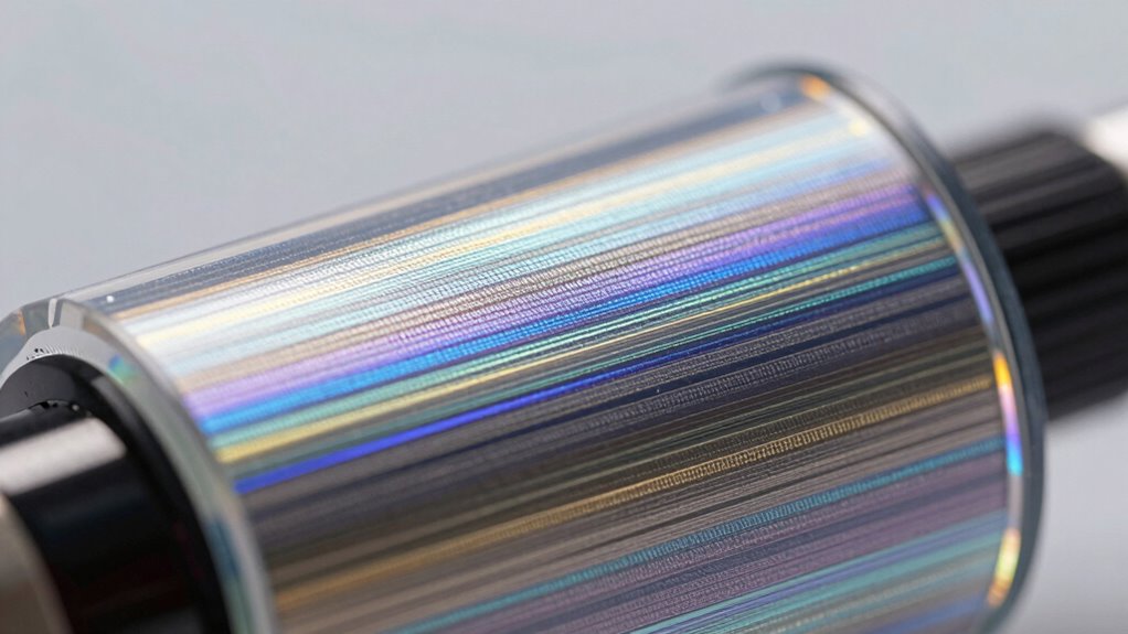
Have you ever wondered how tiny layers at the nanoscale can considerably enhance optical devices? It’s a fascinating area where science meets innovation, and your understanding of these small structures can open a world of improved performance. When you incorporate nano layers into optical systems, you’re leveraging phenomena like quantum confinement and plasmonic enhancement to push the boundaries of what devices can achieve. Quantum confinement occurs when the size of these layers becomes comparable to the wavelength of electrons, effectively trapping them. This confinement alters the electronic and optical properties of the material, allowing for more precise control over light absorption, emission, and transmission. As a result, you get devices with enhanced efficiency, sharper spectral features, and tunable responses. For instance, quantum dots embedded within nano layers can emit specific wavelengths of light, making them ideal for applications like displays, sensors, or laser sources. Additionally, the controllable optical properties enabled by nano layers open up new possibilities for customizing device performance for specific needs. Understanding the material interactions at the nanoscale can further enhance how these layers are engineered for optimal results. Exploring the fabrication techniques used to create uniform nano layers is also crucial for achieving consistent device performance. Moreover, advances in nanomanufacturing methods are continuously improving the precision and scalability of nano layer production.
Plasmonic enhancement is another critical mechanism that comes into play when you add nano layers to optical devices. It involves the excitation of surface plasmons—coherent oscillations of electrons at the interface between a metal and a dielectric. When light interacts with these nano-scale metal layers, it can cause intense local electromagnetic fields, amplifying the light’s intensity in tiny regions. This amplification markedly boosts the device’s sensitivity, making it highly effective in applications like biosensing or surface-enhanced spectroscopy. Plasmonic nano layers can concentrate light into extremely small volumes, which means you get better signal detection, lower power consumption, and potentially faster response times. Exploring these phenomena at the nanoscale reveals how manipulating materials at such small dimensions can lead to significant improvements in device capabilities. These interactions are crucial for designing next-generation optical components with enhanced performance.
By combining quantum confinement effects with plasmonic enhancement, you can tailor optical properties with remarkable precision. For example, layering quantum dots near plasmonic surfaces can amplify their emission, creating highly efficient light sources or sensors. The nano layers enable you to manipulate light at scales much smaller than the wavelength, leading to more compact, efficient, and versatile optical devices. Whether you’re designing better solar cells, more sensitive detectors, or advanced display technologies, understanding and utilizing nano layers can dramatically improve your device’s performance. As research progresses, integrating these phenomena will continue to open new avenues for innovation in optical engineering.
In essence, these tiny layers unlock new capabilities by controlling light in ways that bulk materials simply can’t achieve. Quantum confinement and plasmonic enhancement aren’t just scientific concepts—they’re powerful tools that you can harness to revolutionize optical technology, making devices faster, more efficient, and more adaptable than ever before.
As an affiliate, we earn on qualifying purchases.
Frequently Asked Questions
How Durable Are Nano Layers Under Prolonged Use?
Nano layers are quite durable under prolonged use, but you should watch out for Nano layer degradation over time, which can affect performance. Surface adhesion concerns may also arise, especially if the nano layers aren’t properly applied or maintained. To guarantee longevity, proper handling and protective coatings can help minimize degradation and adhesion issues, extending the lifespan of your devices with nano layers in demanding environments.
Can Nano Layers Be Applied to Flexible or Curved Surfaces?
Yes, nano layers can be applied to flexible substrates and curved surfaces. You can adapt these ultra-thin coatings to bend and conform without cracking or losing functionality. Manufacturers often develop specialized deposition techniques, like atomic layer deposition or sputtering, to guarantee nano layers adhere well and maintain their optical properties on flexible or curved surfaces. This versatility allows for innovative device designs, enhancing performance in flexible electronics and curved optical components.
What Are the Environmental Impacts of Nano Layer Production?
Environmental concerns surround nano layer production, as it can generate waste and involve energy-intensive processes. You need to take into account sustainability practices that minimize harmful impacts, like using eco-friendly materials and reducing chemical usage. By prioritizing sustainable strategies, you help lessen environmental impacts. This careful consideration ensures that nanotechnology advances don’t come at the planet’s expense, aligning innovation with environmental responsibility and promoting greener, cleaner production methods for nano layers.
Are Nano Layers Compatible With Existing Manufacturing Processes?
Nano layers are generally compatible with existing manufacturing processes, especially when considering surface adhesion and manufacturing integration. You can incorporate them into current production lines with minimal modifications, as they often require standard deposition techniques like sputtering or chemical vapor deposition. This ease of integration helps streamline fabrication, ensuring your devices benefit from enhanced optical performance without significant disruptions or the need for entirely new equipment.
How Cost-Effective Are Nano Layers for Large-Scale Production?
Nano layers can be quite cost-effective for large-scale production when you conduct a thorough cost analysis upfront. While initial setup and materials might seem pricey, their scalability helps reduce costs over time. However, you’ll face scalability challenges, such as maintaining uniformity across extensive surfaces. By addressing these challenges early, you can optimize manufacturing processes, making nano layers a viable, economical choice for widespread optical device applications.
plasmonic nano layers for sensors
As an affiliate, we earn on qualifying purchases.
As an affiliate, we earn on qualifying purchases.
Conclusion
Incorporating nano layers into optical devices truly transforms their performance. They enhance light control, reduce losses, and boost efficiency, making your devices smarter and more reliable. Remember, “a chain is only as strong as its weakest link”—and nano layers strengthen every part of your optical system. Embrace this cutting-edge technology, and you’ll see how small changes can lead to big improvements. So, don’t overlook the power of nano layers—they’re the future of optical innovation.
As an affiliate, we earn on qualifying purchases.
As an affiliate, we earn on qualifying purchases.
Fall Picks
fall essentials
As an affiliate, we earn on qualifying purchases.