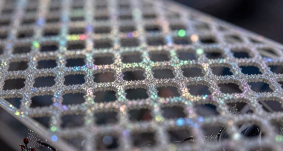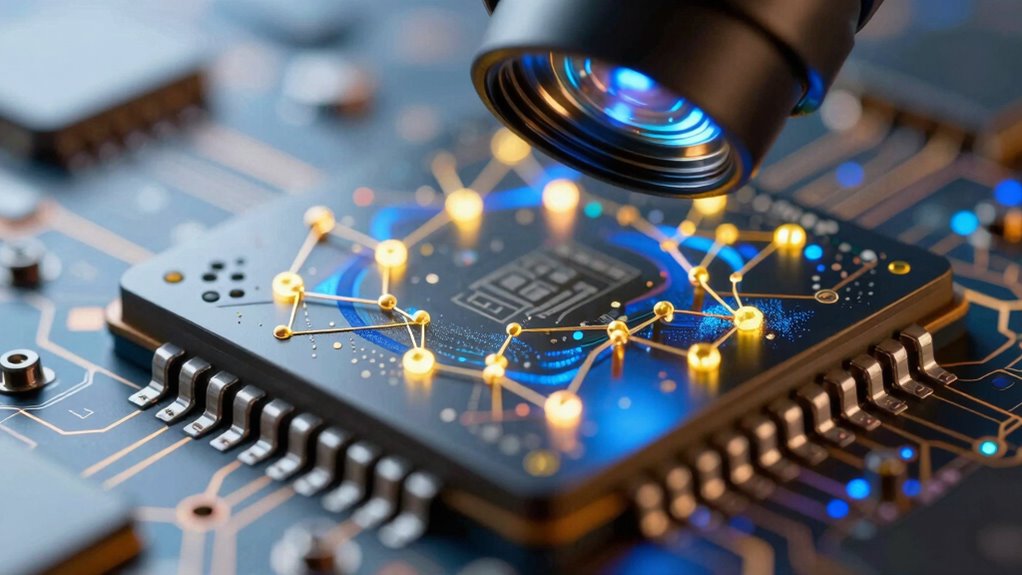

Nanomaterial interfaces directly influence your device’s performance by controlling charge transfer, tunneling, and surface chemistry. When these interfaces are engineered precisely, they reduce energy losses, improve charge mobility, and boost overall efficiency. Variations in interface thickness or chemistry can increase leakage currents or hinder charge flow, impacting speed and reliability. Mastering these nanoscale interactions helps you create more powerful, efficient devices. Keep exploring to uncover how you can optimize interface design for better device outcomes.

Get the latest gadgets delivered free with Prime
- Fast, free delivery on millions of items
- Prime Video, Amazon Music and more included
- Member-only deals all year
Key Takeaways
- Interfaces govern quantum tunneling and charge transfer, directly influencing device conductivity and energy conversion efficiency.
- Surface chemistry at interfaces affects charge mobility, recombination rates, and overall device performance.
- Precise control of interface thickness and properties optimizes tunneling probability and reduces leakage currents.
- Interface engineering enhances charge transfer pathways, boosting device speed and energy storage capabilities.
- Tailoring interfacial chemistry and structure minimizes energy losses, improving device reliability and efficiency.

Nanomaterial interfaces play an essential role in determining the performance and efficiency of modern electronic and energy devices. When you’re working with nanoscale components, the interface between different materials isn’t just a boundary—it’s a dynamic zone where critical processes like quantum tunneling and charge transfer occur. These processes directly influence how well your device functions, impacting everything from conductivity to energy conversion. For instance, the surface chemistry at the interface can significantly alter charge mobility and recombination rates. Quantum tunneling becomes especially important at the nanoscale. Unlike classical particles, electrons don’t need a clear pathway to cross an energy barrier; they can “tunnel” through it. If you’re designing a device like a tunnel diode or a nanostructured transistor, understanding how electrons quantum tunnel across interfaces helps you fine-tune their performance. The thickness and properties of the interface layer determine tunneling probability—making it fundamentally necessary to control these parameters precisely. When tunneling is optimized, electrons pass efficiently, reducing resistance and improving device speed. But if tunneling is uncontrolled or excessive, it can lead to leakage currents, decreasing efficiency and causing energy losses. So, your ability to engineer interfaces that balance tunneling effects is key to high-performance devices. Charge transfer is another essential process happening at nanomaterial interfaces. When electrons move from one material to another, the ease and speed of this transfer dictate how effectively your device operates. For example, in photovoltaic cells or batteries, efficient charge transfer ensures maximum energy conversion and storage. The interface acts as the gatekeeper, where factors like surface chemistry, electronic structure, and interface states influence how readily charges move across boundaries. If you can manipulate these factors—perhaps by functionalizing surfaces or engineering interface layers—you improve charge mobility and reduce recombination or trapping. This directly boosts device efficiency, whether it’s harvesting solar energy or storing electrical power. Additionally, interfacial chemistry can be tailored to enhance or suppress specific charge transfer pathways, providing further control over device behavior. Understanding the fundamental physics at these interfaces enables more precise control over device characteristics. The interplay between quantum tunneling and charge transfer at these interfaces means you need to pay close attention to nanoscale control. Small changes in interface chemistry, structure, or thickness can greatly alter tunneling probabilities and charge mobility. By precisely engineering these interfaces, you can minimize energy losses, increase current flow, and enhance overall device performance. In essence, understanding and controlling the physics at nanomaterial interfaces gives you the ability to push electronic and energy devices to new levels of efficiency and reliability.
nanomaterial interface engineering tools
As an affiliate, we earn on qualifying purchases.
As an affiliate, we earn on qualifying purchases.
Frequently Asked Questions
How Do Environmental Factors Affect Nanomaterial Interface Stability?
Environmental factors like humidity, temperature, and exposure to chemicals can substantially impact nanomaterial interface stability. You’ll see environmental degradation, which weakens the interface over time, and interface oxidation that alters electrical and mechanical properties. These effects can cause performance loss or device failure. To maintain stability, you should consider protective coatings, proper encapsulation, and controlling environmental exposure, ensuring the nanomaterial interfaces remain durable and functional in real-world conditions.
Can Interface Engineering Improve Long-Term Device Durability?
Surface passivation and mechanical adhesion are key to boosting device durability. By engineering interfaces, you can create a barrier that prevents degradation and enhances stability over time. Improving surface passivation minimizes unwanted reactions, while strong mechanical adhesion ensures robust contact, reducing delamination risks. Together, these strategies markedly enhance long-term device performance, ensuring your nanomaterials stay reliable and resilient, even under harsh environmental conditions.
How Do Interface Properties Vary Across Different Nanomaterials?
You’ll find that interface properties vary widely across nanomaterials due to differences in surface chemistry and energy alignment. For example, in some nanomaterials, surface chemistry creates strong bonds, enhancing stability, while others have mismatched energy levels that hinder charge transfer. These variations influence device performance considerably, affecting efficiency, durability, and how well different nanomaterials integrate into complex systems. Understanding these differences helps optimize device design and functionality.
What Are the Challenges in Scaling up Interface Modifications?
Scaling up interface modifications presents challenges like maintaining uniformity during large-scale interface fabrication and ensuring consistent surface passivation across extensive areas. You must control fabrication parameters precisely, avoid defects, and prevent contamination that can disrupt interface properties. Achieving reproducibility and cost-effectiveness also proves tough, requiring advanced techniques and quality assurance. Overcoming these obstacles is key to translating nanoscale interface innovations into reliable, commercial-scale device applications.
How Do Interfaces Influence Device Performance at the Atomic Level?
Interfaces act like busy crossroads at the atomic level, directing the flow of electrons. They influence device performance by controlling quantum tunneling and electron transfer, which can either enhance or hinder efficiency. When you understand how atoms at the interface interact, you can optimize charge movement, reduce energy loss, and improve stability. Mastering these atomic interactions lets you fine-tune devices for better performance, turning tiny interfaces into powerful control points.
quantum tunneling device components
As an affiliate, we earn on qualifying purchases.
As an affiliate, we earn on qualifying purchases.
Conclusion
As you explore nanomaterial interfaces, you’ll realize their power to shape device performance. These tiny boundaries hold secrets that can open unprecedented efficiency and functionality. But the true potential remains just beyond reach, waiting to be fully understood. Will future innovations harness these interfaces to revolutionize technology? Only time will tell, but one thing’s certain—you’re on the brink of uncovering something extraordinary. The next breakthrough could be closer than you think.
charge transfer enhancement materials
As an affiliate, we earn on qualifying purchases.
As an affiliate, we earn on qualifying purchases.
nanostructured transistor components
As an affiliate, we earn on qualifying purchases.
As an affiliate, we earn on qualifying purchases.
Fall Picks
fall essentials
As an affiliate, we earn on qualifying purchases.