

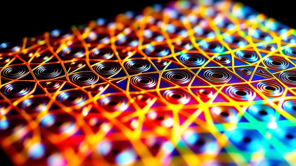
Plasmonic nanostructures harness surface plasmon resonance (SPR) to control light at the nanoscale, creating strong electromagnetic fields that amplify signals for sensing, imaging, and photonics. By designing various shapes like nanoparticles and nanorods, you can tune their resonance to specific wavelengths, enhancing interactions with molecules. Exploring fabrication methods and applications reveals how these structures enable highly sensitive detection techniques. To discover more about their exciting potential and challenges, continue exploring their fascinating world.
Key Takeaways
- Plasmonic nanostructures utilize surface plasmon resonance to generate enhanced electromagnetic fields at the nanoscale.
- The resonance depends on metal type, shape, and size, allowing precise tuning for specific optical applications.
- They enable sensitive detection of molecular interactions through changes in local refractive index.
- Fabrication techniques include top-down lithography and bottom-up chemical synthesis for tailored nanostructures.
- Applications include sensing, imaging, and spectroscopy, leveraging field amplification and resonance tuning for improved performance.
Top picks for "plasmonic nanostructur harness"
Open Amazon search results for this keyword.
As an affiliate, we earn on qualifying purchases.
Understanding Surface Plasmon Resonance in Nanoscale Structures

Surface plasmon resonance (SPR) occurs when conduction electrons on a metal surface oscillate collectively in response to incident light, creating strong electromagnetic fields at the nanoscale. When light hits a metal nanoparticle, these electrons resonate at specific frequencies, amplifying the electromagnetic field near the surface. This resonance depends on factors like the metal type, particle size, and shape, which influence the energy and intensity of the oscillations. As a result, you can detect changes in the local environment—such as molecular binding or refractive index variations—by monitoring shifts in the SPR signal. This sensitivity makes SPR a powerful tool for sensing applications. Understanding how conduction electrons oscillate and generate these intense local fields is essential for designing effective plasmonic devices and sensors. Additionally, ongoing research into AI security helps ensure the safe development and deployment of these advanced nanotechnologies.
Types of Plasmonic Nanostructures and Their Design Principles
Plasmonic nanostructures come in various forms, each designed to optimize the interaction between light and electrons at the nanoscale. You can create nanoparticles, nanorods, shells, or arrays, each with unique properties. The key is to tailor their size, shape, and material to control resonance frequencies and field enhancements. For example, spherical nanoparticles are simple and widely used, while nanorods offer tunable plasmon resonances. To help you decide, here’s a quick comparison:
| Structure | Design Focus | Typical Use |
|---|---|---|
| Spherical NPs | Size for specific resonance | Sensing and imaging |
| Nanorods | Aspect ratio tuning | Surface-enhanced spectroscopy |
Choose structures based on your desired optical properties and application. Additionally, understanding the surface plasmon resonance phenomenon is crucial for designing effective plasmonic nanostructures.
How SPR Enhances Light-Matter Interactions

Surface plasmon resonance (SPR) boosts light-matter interactions by amplifying local electromagnetic fields, making molecules more responsive. You can tune the resonance wavelength to match specific targets, increasing sensitivity and selectivity. This enhancement leads to stronger spectroscopic signals, improving detection capabilities across various applications. Additionally, understanding color accuracy is essential for optimizing signal clarity in spectroscopic measurements.
Localized Field Amplification
Localized field amplification occurs when surface plasmon resonances concentrate electromagnetic energy into tiny regions near nanostructures. This amplification boosts light-matter interactions, enabling numerous applications. Here’s what happens:
- You get intense electric fields that enhance signals in sensing and spectroscopy.
- The amplified fields increase the efficiency of photochemical reactions.
- Localized hotspots improve the sensitivity of biosensors, detecting even single molecules.
- The strong fields can excite nearby quantum dots or dyes, leading to brighter emissions.
These effects happen because nanostructures focus light into small volumes, intensifying the electromagnetic field. This concentrated energy dramatically enhances interactions, making plasmonic nanostructures powerful tools in spectroscopy, sensing, and nanophotonics.
Resonance Wavelength Tuning
Resonance wavelength tuning allows you to precisely control the interaction between light and nanostructures by adjusting their properties so that their surface plasmon resonances align with specific wavelengths. This tuning mainly involves modifying the size, shape, and material composition of the nanostructures, which directly influences their resonance conditions. By doing so, you can shift the plasmon resonance to match desired wavelengths, such as those in the visible or near-infrared spectrum. This control enables you to optimize light absorption, scattering, and energy transfer processes for various applications. When properly tuned, the nanostructure’s plasmonic response becomes highly sensitive to environmental changes, making wavelength tuning a powerful tool for customizing plasmonic behavior to suit specific needs.
Enhanced Spectroscopic Signals
Plasmonic nanostructures considerably amplify light-matter interactions by concentrating electromagnetic fields at their surfaces. This enhancement boosts spectroscopic signals, making detection more sensitive. You can leverage this effect in several ways:
- Surface-Enhanced Raman Scattering (SERS): Signals from molecules are intensified, revealing detailed molecular fingerprints.
- Enhanced Fluorescence: Fluorophores exhibit brighter signals, improving imaging and sensing accuracy.
- Increased Absorption: Light absorption by analytes rises, aiding in trace detection.
- Sensitive Detection: Small changes in the local environment produce measurable spectral shifts.
These effects enable highly sensitive, label-free detection methods, transforming how you analyze biological, chemical, and environmental samples. Harnessing SPR’s ability to amplify spectroscopic signals opens new possibilities in research and diagnostics. Surface plasmon resonance is a key phenomenon underlying these enhancements, allowing precise control of light-matter interactions at the nanoscale.
Fabrication Techniques for Plasmonic Nanostructures

You can create plasmonic nanostructures using top-down fabrication methods like lithography, which allow precise control over size and shape. Alternatively, bottom-up synthesis approaches build structures from atomic or molecular units, offering scalability and simplicity. Understanding these techniques helps you choose the best method for your specific application. Additionally, bedroom decor principles can inspire innovative design approaches for nanostructure assembly, ensuring both functionality and aesthetic appeal.
Top-Down Fabrication Methods
Have you ever wondered how researchers create precisely patterned nanostructures to manipulate light at the nanoscale? Top-down fabrication methods allow you to do just that by starting with bulk materials and sculpting them into nanoscale features. Here are some common techniques:
- Electron Beam Lithography (EBL): Uses focused electron beams to write custom patterns with nanometer precision.
- Focused Ion Beam (FIB) Milling: Employs ion beams to directly etch or modify surfaces with high accuracy.
- Nanoimprint Lithography: Presses a mold into a resist-coated substrate to replicate nanoscale patterns quickly.
- Photolithography: Utilizes light to transfer patterns onto a substrate, suitable for large-scale production.
These methods give you control and precision essential for designing advanced plasmonic nanostructures.
Bottom-Up Synthesis Approaches
Bottom-up synthesis approaches build plasmonic nanostructures by assembling atoms and molecules into desired configurations, often resulting in highly uniform and scalable materials. You can achieve this through methods like chemical reduction, seed-mediated growth, or self-assembly. These techniques enable precise control over size, shape, and arrangement, which is essential for tuning surface plasmon resonance. In these processes, molecules or ions act as building blocks, forming nanostructures under specific conditions. This approach is cost-effective and suitable for large-scale production. Surface plasmon resonance can be finely tuned by adjusting nanostructure geometry and composition, which is a key advantage of bottom-up methods. The table below summarizes key methods and their characteristics:
| Method | Key Features | Typical Applications |
|---|---|---|
| Chemical reduction | Simple, scalable, produces nanoparticles | Sensing, imaging |
| Seed-mediated growth | Precise shape control | Catalysis, photothermal therapy |
| Self-assembly | Bottom-up organization | Sensors, waveguides |
Applications of Plasmonic Nanostructures in Sensing and Imaging

Plasmonic nanostructures have revolutionized sensing and imaging technologies by enabling highly sensitive detection of biological, chemical, and environmental analytes. You can leverage their unique properties in several ways:
Plasmonic nanostructures enable ultra-sensitive detection for advanced sensing and imaging applications.
- Surface-enhanced Raman scattering (SERS): Amplifies signals for detecting trace molecules with high specificity.
- Localized surface plasmon resonance (LSPR) sensors: Monitor changes in refractive index, allowing real-time detection.
- Colorimetric assays: Use visible color changes for quick, on-site analysis.
- Bioimaging: Enhance contrast and resolution in cellular and tissue imaging.
– Additionally, understanding the best anime movies can inspire innovative visual techniques in imaging applications.
These applications enable faster, more accurate diagnostics and environmental monitoring, transforming how you detect and visualize minute analytes with precision and ease.
Challenges and Future Directions in Plasmonic Research

Despite significant advancements, several challenges still hinder the full potential of plasmonic nanostructures. One major issue is fabrication precision; creating uniform, scalable nanostructures remains difficult, affecting reproducibility and performance. Additionally, plasmonic losses, mainly from metal absorption, limit efficiency and signal strength. Stability is another concern—metal nanoparticles can degrade over time or under harsh conditions, reducing their longevity. You also face challenges in designing tunable systems that work across broad wavelengths for diverse applications. Future research must focus on overcoming these obstacles by developing advanced fabrication techniques, exploring new materials like aluminum or graphene, and enhancing stability through protective coatings. Moreover, understanding the industry trends and ongoing innovations in the field will be crucial in advancing plasmonic technologies. Addressing these issues will liberate new possibilities and expand plasmonics’ role in next-generation technologies.
Integrating Plasmonics With Other Nanoscale Technologies

Integrating plasmonics with other nanoscale technologies offers a promising pathway to enhance device capabilities and open new functionalities. This fusion enables you to develop innovative systems with improved sensitivity, speed, and miniaturization. Here are four key approaches:
Harnessing plasmonics with nanoscale tech unlocks new functionalities and boosts device performance.
- Combining plasmonics with nanophotonics for ultra-compact optical circuits.
- Merging plasmonic structures with quantum dots to boost light-matter interactions.
- Integrating plasmonics with nanoscale sensors for real-time, high-precision detection.
- Coupling plasmonic devices with 2D materials like graphene to enhance tunability and performance.
Additionally, advancements in surface plasmon resonance techniques can further improve sensing accuracy and device responsiveness.
These integrations allow you to push the boundaries of current nanotechnology, creating smarter, faster, and more versatile applications across sensing, imaging, and communication.
Frequently Asked Questions
How Do Environmental Factors Influence Plasmon Resonance Stability?
Environmental factors like temperature, pH, and surrounding medium markedly impact plasmon resonance stability. You might notice shifts in resonance wavelength or signal intensity as these conditions change, affecting your measurements. Variations in the refractive index of the environment can cause resonance peaks to drift, reducing accuracy. To maintain stability, you should carefully control environmental conditions or implement surface modifications that enhance resistance to these external influences.
What Are the Cost Implications of Large-Scale Plasmonic Nanostructure Production?
You’ll find that large-scale production of plasmonic nanostructures can be costly due to the need for precise fabrication techniques and high-quality materials. Equipment investments and maintaining strict process controls add to expenses. However, scaling up can reduce per-unit costs over time, making mass production more feasible. Careful planning and technological advancements help balance initial costs with long-term benefits in applications like sensing and imaging.
Can Plasmonic Nanostructures Be Used in Biological Applications Without Toxicity?
Did you know that over 60% of nanomaterials are being explored for biomedical applications? You can definitely use plasmonic nanostructures in biological settings without toxicity, but it depends on their composition and surface modifications. You should choose biocompatible materials like gold or silver and make certain of proper coating to reduce adverse effects. Proper testing and regulatory approval are essential before clinical use to ensure safety and effectiveness.
How Do Different Substrates Affect Plasmonic Performance?
Different substrates markedly influence your plasmonic performance. If you choose a substrate with a high refractive index, you’ll notice shifts in resonance frequency, potentially enhancing sensitivity. Conversely, a substrate with poor conductivity or roughness can dampen plasmonic signals, reducing effectiveness. To optimize your results, select substrates like glass or metallic films that match your desired resonance and minimize losses, ensuring strong, clear plasmonic responses for your application.
What Are Emerging Trends in Tunable and Reconfigurable Plasmonic Devices?
Did you know that the market for tunable plasmonic devices is expected to grow at a CAGR of over 20% by 2030? You’ll see emerging trends focusing on dynamic reconfigurability using phase-change materials, liquid crystals, and microelectromechanical systems (MEMS). These innovations let you actively control plasmonic responses in real-time, enabling advanced sensors, smart imaging, and adaptive photonic circuits that revolutionize how you manipulate light at the nanoscale.
Conclusion
Harnessing surface plasmon resonance is like opening a gateway to a world where light dances at your fingertips. By mastering nanostructure design and fabrication, you can amplify light-matter interactions, transforming sensing and imaging. Though challenges remain, the future of plasmonics shines brightly—your innovations will carve pathways through this shimmering landscape. Embrace these tiny titans of light, and watch them illuminate new horizons in nanotechnology.