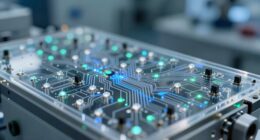

Photonic chips use light instead of electrons to process data, enabling faster speeds and lower energy use than traditional electronics. They consist of waveguides, lasers, and detectors made from advanced materials like lithium niobate and InP. Recent breakthroughs have led to chips that perform complex tasks at unprecedented speeds, with manufacturing still evolving to overcome integration challenges. If you want to discover how these innovations are shaping future technology, there’s more to explore.
Key Takeaways
- Photonic chips use light instead of electrons, enabling faster data transmission at near-light speeds for computing applications.
- Advances in materials like lithium niobate and InP improve efficiency and scalability of photonic components.
- Manufacturing challenges include precise nanolithography and hybrid integration of diverse materials for high-density chips.
- Breakthroughs such as China’s CHIPX and Columbia’s 3D photonic-electronic chips demonstrate significant speed and bandwidth improvements.
- Ongoing innovations aim to overcome fabrication hurdles, expanding photonic computing’s role in high-performance, energy-efficient systems.

KEEP COMPUTING: How Light Solves Computing's Impossible Problem
As an affiliate, we earn on qualifying purchases.
As an affiliate, we earn on qualifying purchases.
The Foundations of Photonic Chip Technology

To understand photonic chip technology, you need to grasp how photons replace electrons in data processing and transmission. Unlike electrons, photons move at near the speed of light, enabling faster data flow with less latency. Photonic chips use tiny waveguides—etched optical paths—to direct light precisely across the chip. Modulators encode information by changing the light’s intensity, phase, or frequency, while photodetectors convert the optical signals back into electrical signals for processing. Lasers serve as the initial light source, either integrated into the chip or coupled externally. These components work together to transmit data efficiently, with minimal energy loss and interference. The integration of photonic components into existing electronic systems is a crucial step toward high-performance computing. Advances in waveguide design and materials science are continuously improving the efficiency and scalability of photonic chips, making them more viable for mainstream applications. Additionally, research into sustainable materials is helping to reduce the environmental impact of photonic manufacturing, which further supports their commercial viability. Understanding these fundamental parts helps you appreciate how photonics can revolutionize computing speeds and capabilities.

Linshang LS116 Optical Transmission VLT Tester Light Transmittance Meter with 380-760nm White Visible Light Meet CIE Standard
1. The light transmittance meter adopts the parallel light path of the light source and the light collecting…
As an affiliate, we earn on qualifying purchases.
As an affiliate, we earn on qualifying purchases.
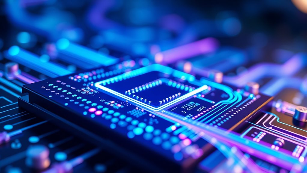
Benefits Over Traditional Electronic Systems

Photonic chips outperform traditional electronic systems by operating at speeds near that of light, which considerably reduces data transmission latency. This means your data moves faster, improving overall system performance. With photonic technology, you benefit from:
- Lower Latency: Light-speed data transfer minimizes delays, making real-time processing more achievable.
- Reduced Heat: Photons encounter less resistance than electrons, resulting in less heat generation and better energy efficiency.
- Higher Bandwidth: Multiple light channels allow parallel data streams, boosting capacity without increasing physical size.
These advantages lead to faster, more efficient computing systems that can handle complex tasks with ease. By replacing electrons with photons, you access a new level of speed and performance, especially in data-heavy applications like AI, big data, and high-performance computing.

Cruiser 1×4 PLC Optical Splitter Cassette, Planar Waveguide Optical Splitter, 1 Sub-4 Fiber Optic Splitter
Low insertion loss, Low PDL and High reliability
As an affiliate, we earn on qualifying purchases.
As an affiliate, we earn on qualifying purchases.
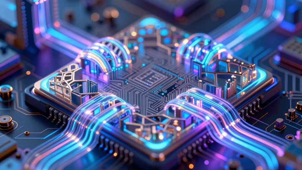
Core Components and Material Innovations

The core components of photonic chips—such as waveguides, lasers, modulators, and detectors—are essential for guiding, encoding, and decoding light signals with high efficiency. Waveguides direct photons precisely along the chip’s surface, while lasers generate the initial light source, either integrated or external. Modulators encode data by altering light’s phase, intensity, or frequency, enabling high-speed information transfer. Detectors convert optical signals back into electrical form for processing. Material innovations play a critical role: thin-film lithium niobate offers low optical loss and signal stability, and indium phosphide (InP) supports integrating active functions like amplification. Microscopic resonators with phase-change materials enable light-based memory, pushing the limits of miniaturization. These components and materials collectively drive the advancement of faster, more efficient photonic systems. Vetted

Ferwooh 5PCS Laser Sensor Module Non-Modulator Tube Receiver Output High Level + 5PCS KY-008 650nm Laser Sensor Module
【Laser Sensor Module】Size: 1.52CM * 2.22CM; Power supply voltage: 5V;Output:When the laser output it's High level; when no…
As an affiliate, we earn on qualifying purchases.
As an affiliate, we earn on qualifying purchases.
Recent Breakthroughs and Leading Developments
Recent breakthroughs are pushing photonic chip performance to new heights, with China’s CHIPX chip achieving 1,000-fold improvements in complex computing tasks. Industry leaders like Columbia Engineering are developing 3D photonic-electronic chips that reach 800 Gb/s bandwidth for AI applications. These innovations are transforming the landscape, making ultra-fast, energy-efficient computing more accessible than ever. As research continues, the integration of light-based technologies promises to revolutionize the speed and efficiency of future computing systems.
Breakthroughs in Chip Performance
Advances in photonic chip technology are pushing performance boundaries, enabling faster, more efficient data processing than ever before. You can now see breakthroughs like these:
- The CHIPX chip from China achieves 1,000-fold improvements in complex computing tasks, dramatically boosting speed.
- Columbia Engineering’s 2025 3D photonic-electronic chip reaches 800 Gb/s bandwidth, enhancing AI and data transfer rates.
- Production of 12,000 lithium niobate wafers annually supports high-density integration and scalable manufacturing.
These developments mean you benefit from lower latency, reduced heat, and increased energy efficiency. They also pave the way for compact, powerful systems capable of handling massive data loads. Such progress accelerates the evolution of high-performance computing, making light-speed processing a real-world reality.
Leading Industry Innovations
Innovations in photonic chip technology are transforming the industry by introducing breakthroughs that dramatically boost processing speed and efficiency. You’ll see China’s CHIPX chip achieving 1,000-fold improvements in complex computing tasks, pushing the limits of data processing. Columbia Engineering’s 2025 3D photonic-electronic chip reaches 800 Gb/s bandwidth, enabling faster AI computations. Production lines now manufacture 12,000 thin-film lithium niobate wafers annually, supporting scalable manufacturing. Monolithic integration allows high optical density, reducing size and power consumption. Hybrid architectures address bottlenecks in AI data transfer, enhancing performance. These innovations make photonic chips viable for diverse applications like data centers, biomedical devices, and autonomous systems. Industry leaders are also refining fabrication processes, combining photonics with CMOS technology to improve compatibility and integration, setting new standards for high-speed, energy-efficient computing.
Manufacturing Processes and Integration Challenges

You need to understand that material compatibility issues can complicate manufacturing, as integrating diverse components like lasers, modulators, and detectors requires precise material choices. Achieving the necessary accuracy in photolithography is critical, but maintaining such precision across large wafers remains a challenge. Additionally, hybrid integration faces hurdles in seamlessly combining photonic and electronic systems without compromising performance or yield. Ensuring material compatibility throughout the process is essential for reliable device fabrication and long-term operation. Moreover, manufacturing scalability becomes increasingly difficult as the complexity of the integrated systems grows, demanding innovative solutions to keep pace with technological advancements.
Material Compatibility Issues
Material compatibility remains a major challenge in manufacturing photonic chips, as integrating diverse materials such as silicon, lithium niobate, and indium phosphide often leads to complex fabrication processes. You face issues like differing thermal expansion rates, which can cause stress and defects. Managing lattice mismatches requires precise bonding techniques to prevent cracks and optical losses. Additionally, aligning material properties is critical for device performance; mismatched refractive indices or incompatible fabrication steps can impair signal quality. To address these challenges, you must:
- Develop hybrid integration methods that combine different materials without compromising integrity.
- Optimize bonding processes to ensure stability and minimal optical loss.
- Fine-tune fabrication parameters to accommodate material-specific characteristics, ensuring seamless device operation.
- Implement data-driven comparisons to evaluate material performance and compatibility, guiding optimal integration strategies. Furthermore, understanding material compatibility at a fundamental level can help anticipate potential issues before fabrication, saving time and resources. Incorporating material characterization techniques can provide deeper insights into how different materials interact during manufacturing, leading to improved outcomes. Additionally, advances in materials science research are essential for discovering new compatible material combinations that can simplify fabrication processes and enhance device performance. Recognizing the importance of thermal properties in material selection can also mitigate stress-related defects during operation.
Precision in Photolithography
How do manufacturers achieve the nanometer-scale precision required for photolithography in photonic chip production? You rely on advanced lithography tools like deep ultraviolet (DUV) and extreme ultraviolet (EUV) systems, which use very short wavelengths of light to create fine patterns. Precise alignment techniques ensure each layer matches perfectly, minimizing errors. You must control environmental factors such as temperature, vibrations, and airborne particles, as even minor disturbances can affect accuracy. High-resolution masks guide the light exposure, defining the tiny features on the wafer. You also employ sophisticated resist materials that develop sharply, enabling pattern transfer at nanometer scales. Regular calibration and real-time monitoring further enhance accuracy, guaranteeing consistent patterning across large wafers. Maintaining this precision is crucial for integrating complex optical components on photonic chips.
Hybrid Integration Challenges
Integrating diverse materials such as lithium niobate, indium phosphide, and silicon into a single photonic chip presents significant manufacturing challenges. First, aligning different material properties requires precise fabrication techniques, as each material responds differently to processes like etching and deposition. Second, ensuring seamless interfaces between dissimilar layers is critical; mismatches can cause signal loss or device failure. Third, integrating active components like lasers and detectors with passive waveguides demands complex hybrid assembly, often involving multiple fabrication steps. You must also manage thermal expansion differences and material stresses, which can degrade performance. Overcoming these challenges involves advanced process control, innovative bonding methods, and meticulous quality assurance to produce reliable, high-performance hybrid photonic chips.
Diverse Applications Transforming Multiple Industries

Diverse industries are rapidly adopting photonic chips to revolutionize their processes and capabilities. In aerospace, they enable faster data transmission for navigation and communication systems, improving safety and efficiency. In biomedicine, photonic chips power advanced imaging, real-time diagnostics, and lab-on-chip devices, accelerating research and patient care. Financial firms leverage these chips for ultra-fast trading algorithms and risk analysis, gaining a competitive edge. Data centers benefit from increased bandwidth and reduced latency, supporting cloud computing and AI workloads. Automotive industries integrate photonic sensors for autonomous driving and vehicle safety. Researchers also use them for molecular simulations, materials discovery, and environmental monitoring. The versatility of photonic chips transforms these sectors by delivering high-speed, energy-efficient solutions that push technological boundaries and release new possibilities. High-speed data transmission is a key factor driving the adoption of photonic technology across these fields. Additionally, the integration of photonic materials is enhancing the performance and durability of these chips in demanding environments. Furthermore, innovations in nanotechnology are enabling even more compact and efficient chip designs, broadening their application spectrum. A focus on cybersecurity is essential to protect the sensitive data transmitted through these high-speed systems, ensuring secure communications across industries.
Frequently Asked Questions
How Do Photonic Chips Compare in Cost to Traditional Electronic Chips?
You’ll find that photonic chips are currently more expensive than traditional electronic chips, mainly because of the complex manufacturing processes and specialized materials involved. However, their high performance, low heat, and energy efficiency can offset initial costs over time, especially in high-demand applications like data centers and AI. As production scales up and technology advances, expect the costs to decrease, making photonic chips more economically competitive.
What Are the Main Obstacles to Large-Scale Commercial Adoption?
The main obstacles to large-scale commercial adoption include integrating diverse materials for lasers, modulators, and detectors, which complicates manufacturing. You also face challenges in scaling production efficiently and cost-effectively, since current fabrication processes are complex and expensive. Additionally, ensuring compatibility with existing electronic systems requires advanced hybrid integration techniques. Overcoming these technical and economic hurdles is vital for widespread adoption of photonic chips in various industries.
How Does Thermal Management Differ in Photonic Versus Electronic Systems?
Did you know photonic chips generate up to 90% less heat than electronic ones? You’ll find thermal management in photonic systems simpler because light transmission produces minimal heat, reducing cooling needs. In contrast, electronic systems struggle with heat dissipation from resistance, requiring complex cooling solutions. So, with photonic chips, you can expect more efficient operation, less energy waste, and easier thermal control, making them ideal for high-speed, high-density computing environments.
Can Photonic Chips Be Integrated With Existing Electronic Infrastructure Easily?
Yes, you can integrate photonic chips with existing electronic infrastructure relatively easily. They’re designed to be compatible with CMOS processes, making hybrid systems feasible. You’ll find that photonic components like waveguides and lasers can be incorporated alongside electronic circuits, enabling high-speed data transfer and processing without major redesigns. However, challenges remain in seamlessly merging different materials and ensuring efficient communication between photonic and electronic parts.
What Are the Environmental Impacts of Manufacturing Photonic Chips?
You might think manufacturing photonic chips is eco-friendly, but it’s quite complex. While they generate less heat and energy during use, their production involves energy-intensive processes like lithography and material synthesis, which can produce significant waste and emissions. Additionally, sourcing rare materials like indium phosphide impacts resource sustainability. Balancing these environmental impacts requires careful consideration, innovation, and cleaner manufacturing techniques to truly minimize ecological footprints.
Conclusion
You might think photonic chips are still too experimental for real-world use, but advancements prove otherwise. Their speed and efficiency can revolutionize everything from computing to healthcare, making devices faster and more energy-efficient. Don’t overlook their potential—it’s not just future tech, it’s here to transform your industry today. Embrace photonics now, or risk falling behind in a rapidly evolving digital world. The future of computing is happening at the speed of light.