
Nanoelectronics push device limits by harnessing quantum tunneling, allowing electrons to pass through barriers beyond classical physics, which increases speed and reduces energy use. They also benefit from materials with high electron mobility, like graphene, enabling faster, more efficient devices. Advances in material science and atomic-scale engineering help optimize these effects, supporting continued miniaturization. If you keep exploring, you’ll uncover how these innovations are shaping the future of electronics far beyond tradition.
Key Takeaways
- Quantum tunneling enables electrons to bypass classical barriers, allowing faster switching and reduced energy consumption in nanoscale devices.
- High electron mobility in materials like graphene enhances device speed and efficiency beyond traditional silicon-based technology.
- Advances in material science and atomic-scale engineering optimize electronic properties for ultra-miniaturized components.
- Quantum confinement effects are exploited to tailor electronic behavior, pushing device performance past conventional limits.
- Integrating quantum effects and novel materials fosters innovative, energy-efficient, and high-speed nanoelectronic devices.
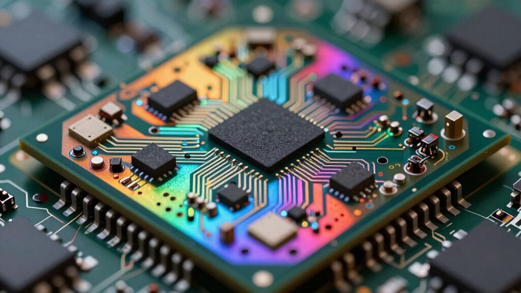
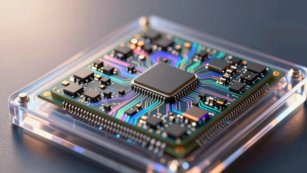
As devices continue to shrink at the nanoscale, researchers are revealing new possibilities for electronics performance and efficiency. One of the key phenomena they explore is quantum tunneling, which occurs when electrons pass through barriers that classical physics would deem impenetrable. While this might seem like a challenge—causing leakage currents and potential device failure—it also liberates innovative ways to design ultra-compact components. You might think of quantum tunneling as a kind of shortcut that electrons take, enabling faster switching and reducing energy consumption. This effect becomes especially significant as transistors approach atomic dimensions, where traditional semiconductor physics no longer fully applies. By understanding and controlling quantum tunneling, you can push device performance beyond conventional limits, making electronics smaller, faster, and more energy-efficient. The ability to manipulate such quantum effects is central to advancing nanoelectronic device technology. Electron mobility, another essential factor, plays a key role in nanoelectronics. It determines how quickly electrons can move through a material when an electric field is applied. Higher electron mobility means your devices can operate at higher speeds with less power dissipation. As you scale down to the nanoscale, materials like graphene and transition metal dichalcogenides show exceptional electron mobility, outperforming traditional silicon. This allows for faster transistors and more efficient circuits. You can leverage these materials to design devices that not only perform better but also consume less energy, addressing the growing demand for portable and energy-efficient electronics. The challenge lies in maintaining high electron mobility at such small scales, but advances in material science and fabrication techniques are making this increasingly feasible. Additionally, understanding the impact of quantum confinement effects is crucial for optimizing device performance at the nanoscale. Exploring material science further helps in discovering new compounds with tailored properties for nanoelectronics. Recognizing the importance of atomic-scale engineering can accelerate the development of innovative nanoelectronic components. The interplay between quantum tunneling and electron mobility shapes the future of nanoelectronics. You can think of quantum tunneling as both a hurdle and an opportunity—something to manage carefully while also exploiting it for novel functionalities. Meanwhile, improving electron mobility ensures that electrons can traverse tiny structures quickly and efficiently. Together, these phenomena enable the development of devices that break through traditional limits, offering unprecedented speed, miniaturization, and energy savings. As you embrace these principles, you contribute to a new era of electronics, where the boundaries of what’s possible continue to expand at the nanoscale. The ongoing research and innovation in this field promise to redefine the capabilities of future technologies, making your devices smarter, faster, and more efficient than ever before.

Graphene Nanoelectronics: Metrology, Synthesis, Properties and Applications (NanoScience and Technology)
As an affiliate, we earn on qualifying purchases.
As an affiliate, we earn on qualifying purchases.
Frequently Asked Questions
How Does Nanoelectronics Impact Environmental Sustainability?
Nanoelectronics positively impact environmental sustainability by enabling the use of eco-friendly materials and improving resource efficiency. You benefit from smaller, energy-efficient devices that consume less power, reducing your carbon footprint. By integrating nanoelectronics, manufacturers can create sustainable products that require fewer raw materials and generate less waste. This innovation helps conserve resources, lowers environmental impact, and promotes a greener future, making your technology choices more eco-conscious and sustainable.
What Are the Safety Concerns With Nanoelectronic Manufacturing?
Nanoelectronics manufacturing is a double-edged sword, with safety concerns lurking like shadows. You should be aware of nano safety issues, as tiny particles can pose health risks if inhaled or come into contact with skin. Manufacturing hazards include exposure to hazardous chemicals and the potential release of nanoparticles. Proper protective measures and handling protocols are vital to prevent accidents and guarantee safe production, keeping both workers and the environment protected.
Can Nanoelectronics Be Integrated With Existing Device Technologies?
Yes, nanoelectronics can be integrated with existing device technologies. You’ll find that quantum confinement effects enable these tiny components to operate efficiently within current systems. Material compatibility is essential, ensuring that nanoelectronic materials seamlessly blend with traditional semiconductors. By addressing these factors, you can enhance device performance while maintaining manufacturing practicality, allowing nanoelectronics to complement and extend the capabilities of existing technologies effectively.
How Does Nanoelectronics Influence Energy Consumption in Devices?
Nanoelectronics profoundly influence energy consumption in devices by enhancing energy efficiency and improving power management. You’ll notice that smaller components require less power, reducing overall energy use. Nano-scale transistors and circuits enable devices to operate with minimal energy wastage, extending battery life and lowering energy costs. These advancements allow devices to perform better while consuming less power, making them more sustainable and cost-effective in the long run.
What Are the Future Challenges in Scaling Nanoelectronic Components?
Scaling nanoelectronic components is like traversing a tightrope over a stormy sea, with quantum tunneling and material miniaturization as constant obstacles. Future challenges include controlling quantum effects that become unpredictable at tiny scales and developing new materials that maintain stability and performance. You’ll need innovative fabrication techniques and precise engineering to overcome these hurdles, ensuring devices continue to shrink without losing efficiency or reliability.

High-k Gate Dielectric Materials
As an affiliate, we earn on qualifying purchases.
As an affiliate, we earn on qualifying purchases.
Conclusion
As you explore the future of nanoelectronics, you’ll find that these tiny innovations gently nudge the boundaries of what’s possible, opening doors to even more exciting advancements. While challenges remain, the subtle progress in this field promises a horizon filled with smarter, faster devices that seamlessly integrate into your life. Embrace the journey, knowing that each small step quietly paves the way for a more connected and efficient tomorrow.

Handbook for III-V High Electron Mobility Transistor Technologies
As an affiliate, we earn on qualifying purchases.
As an affiliate, we earn on qualifying purchases.
Kyuionty Engineer Scale Ruler 12 Inch, Aluminum Laser-Etched Triangular Drafting Tool for Civil Engineering Drafting, Imperial Scale 1:10, 1:20, 1:30, 1:40, 1:50, 1:60 (Blue)
Package Content: 1 x Engineering Scale Ruler 12 Inch with PVC Packing Box.
As an affiliate, we earn on qualifying purchases.
As an affiliate, we earn on qualifying purchases.