Nano-enhanced surfaces boost your device sensitivity by increasing the surface area that interacts with target molecules or signals. This expansion amplifies detection capabilities and allows for more precise sensing of low-concentration substances. Surface nanostructures also enable stronger, more specific interactions, making devices more responsive to subtle environmental changes. Combining fabrication and surface functionalization creates surfaces that are highly reactive and selective. To understand how these advancements work together, keep exploring further insights.
Key Takeaways
- Nanostructures increase surface area, allowing more interaction with target molecules and signals.
- Surface functionalization adds specific chemical groups, enhancing selective recognition of analytes.
- Nano-enhanced surfaces amplify signals through phenomena like surface plasmon resonance.
- Precise control over nanostructure dimensions optimizes sensitivity and response times.
- The synergy of fabrication and functionalization enables detection of low-concentration or subtle environmental changes.
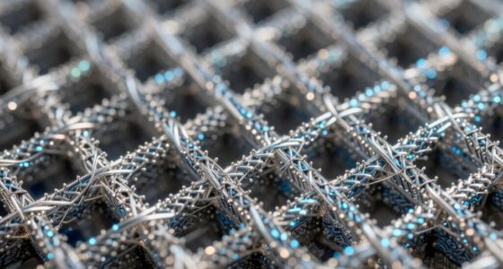
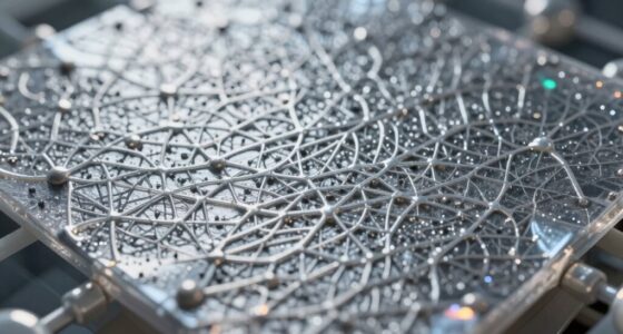
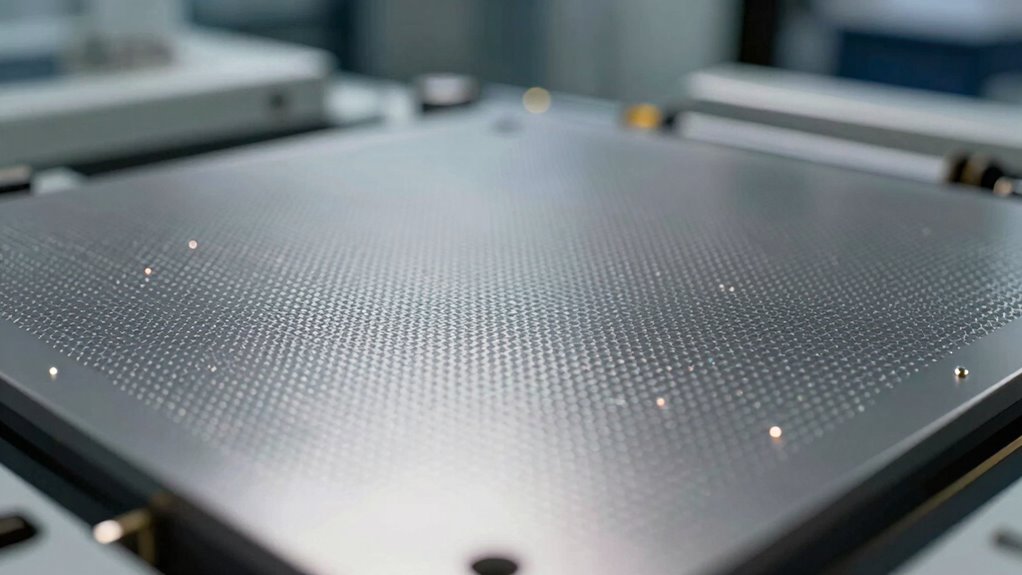
Advancements in nanotechnology are transforming how devices detect and respond to their environment, with nano-enhanced surfaces playing a critical role. These surfaces leverage carefully designed nanostructures to improve sensitivity and performance. At the core of this progress is nanostructure fabrication, a process that creates intricate, nanoscale patterns on surfaces. By manipulating materials at such a small scale, you can considerably increase the surface area, which enhances the device’s ability to interact with molecules, particles, or signals in its environment. This increased interaction capacity means that sensors, for example, can detect lower concentrations of chemical or biological agents more quickly and accurately than ever before. Additionally, understanding the importance of contrast ratio can help in optimizing sensor responses in various environments.
Surface functionalization techniques further boost these capabilities by adding specific chemical groups or coatings to the nanostructures. These techniques allow you to tailor the surface properties to target particular molecules or signals. For instance, by attaching antibodies or other recognition elements through surface functionalization, you make your device highly selective, reducing false positives and increasing reliability. This process also improves the adhesion of nanomaterials to the substrate, guaranteeing durability and consistent performance over time. Moreover, ongoing research into nanostructure design can lead to even more effective ways to amplify sensor responses. In addition, advancements in surface chemistry are continually refining how these functionalizations are achieved, leading to more robust and versatile sensor surfaces.
When you combine nanostructure fabrication with effective surface functionalization, you create surfaces that are both highly reactive and selectively responsive. This synergy enables your device to detect subtle changes in its surroundings, which is essential in applications like medical diagnostics, environmental monitoring, and industrial process control. The nanostructures enhance the physical interaction with target molecules, while surface functionalization ensures that these interactions are specific and meaningful. As a result, your device becomes more sensitive, capable of recognizing signals that would otherwise be too weak to detect. Furthermore, exploring different nanofabrication techniques can help optimize the design for specific sensing needs.
In practical terms, this means faster response times, higher detection limits, and improved overall efficiency. You can fine-tune the nanostructure dimensions and surface chemistry to optimize sensitivity for your particular application. For example, creating nanostructures with specific geometries can amplify signals through phenomena like surface plasmon resonance or localized electric field enhancement. Meanwhile, surface functionalization can be customized to bind tightly with target analytes, ensuring that your device is both precise and reliable. The ongoing development of new nanofabrication techniques continues to expand the possibilities for customizing these surfaces further.
Ultimately, the combination of nanostructure fabrication and surface functionalization techniques opens new frontiers in device sensitivity. You gain the ability to develop smarter, more responsive tools that can operate effectively even in complex or low-concentration environments. This technological leap not only improves existing sensors but also paves the way for innovative applications across multiple fields, making your devices more efficient, accurate, and adaptable.
HiLetgo 5pcs Nano I/O Expansion Sensor Shield for Arduino UNO R1 Nano 3.0 Duemilanove 2009
14 I/O Pin (servo type with GND, power and signal)
As an affiliate, we earn on qualifying purchases.
As an affiliate, we earn on qualifying purchases.
Frequently Asked Questions
How Durable Are Nano-Enhanced Surfaces Under Long-Term Use?
Nano-enhanced surfaces are generally quite durable, but their long-term stability depends on nanoparticle stability and surface wear. You might notice some degradation over time if particles detach or surface wear occurs due to constant use. However, with proper design and protective coatings, these surfaces can sustain their functionality longer. Regular maintenance can also help guarantee the durability and consistent performance of nano-enhanced devices in the long run.
Are Nano-Enhanced Surfaces Cost-Effective for Large-Scale Manufacturing?
Nano-enhanced surfaces can be cost-effective for large-scale manufacturing when you conduct a thorough cost analysis and consider market scalability. Although initial setup costs may be higher, their enhanced sensitivity can reduce overall device costs by improving performance and longevity. As production volumes increase, economies of scale kick in, lowering per-unit costs, making these surfaces a viable option for mass production, especially in high-demand sectors like healthcare and electronics.
Can Nano-Enhanced Surfaces Be Integrated With Existing Device Technologies?
Yes, you can integrate nano-enhanced surfaces with existing device technologies through surface functionalization, which modifies surfaces at the nanoscale to improve performance. By applying nano fabrication techniques, you effectively add or modify features on current devices, enhancing sensitivity and functionality. This process is adaptable and can be tailored to your device specifications, making integration feasible without overhauling your entire system.
Do Nano-Enhanced Surfaces Pose Environmental or Health Risks?
Nano-enhanced surfaces can pose environmental safety and health implications if not properly managed. You should handle these materials with care, avoiding inhalation or skin contact, as nanoparticles may be toxic or cause unforeseen environmental damage. It’s vital to follow safety guidelines and conduct thorough risk assessments. Researchers must guarantee safe disposal and containment to minimize potential risks, safeguarding both human health and the environment.
How Do Nano-Structured Surfaces Compare With Other Sensitivity Enhancement Methods?
Imagine tuning a musical instrument, where nano-structured surfaces act like finely adjusted strings. Compared to other methods, they excel in surface functionalization, offering precise control over interactions at the nanoscale. This leads to superior signal amplification, making your devices more sensitive and accurate. Unlike bulk modifications, nano-structured surfaces provide a tailored, efficient approach, transforming subtle signals into clear, measurable responses, much like a well-tuned instrument producing harmonious sound.
surface functionalization kits for sensors
As an affiliate, we earn on qualifying purchases.
As an affiliate, we earn on qualifying purchases.
Conclusion
By harnessing nano-enhanced surfaces, you reveal a new realm of device sensitivity, turning ordinary tools into extraordinary sensors. These surfaces are like a finely tuned orchestra, where each nanostructure plays a vital role in amplifying signals and detecting even the faintest whispers. As you embrace this technology, you’re not just improving devices—you’re igniting a revolution that makes the invisible visible, opening doors to discoveries that can change lives forever.

Nanoscale Fabrication, Optimization, Scale-up and Biological Aspects of Pharmaceutical Nanotechnology
As an affiliate, we earn on qualifying purchases.
As an affiliate, we earn on qualifying purchases.

Surface Plasmon Resonance Sensors: A Materials Guide to Design and Optimization (SpringerBriefs in Physics)
As an affiliate, we earn on qualifying purchases.
As an affiliate, we earn on qualifying purchases.