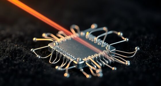

Nanofabrication via Atomic Layer Deposition (ALD) involves using atomic-scale, self-limiting surface reactions to deposit ultra-thin, uniform films with high precision. This process enables you to create complex nanostructures with excellent consistency, essential for advanced electronics, coatings, and materials. ALD’s versatility with materials like metal oxides and nitrides makes it widely applicable. To discover how ALD overcomes challenges and shapes future nanotechnology, keep exploring further.
Key Takeaways
- ALD enables the precise, atomic-scale fabrication of uniform, conformal thin films essential for advanced nanostructures.
- The process uses sequential, self-limiting surface reactions, ensuring high accuracy and consistency on complex nanofabrication surfaces.
- Material selection and precursor handling are critical for safe, effective nanofabrication, with options including metal oxides and nitrides.
- Overcoming scalability, process speed, and environmental challenges is vital for industrial adoption of ALD in nanofabrication.
- Future advancements include nanoscale patterning, 3D nanostructure development, and eco-friendly processes, expanding nanofabrication capabilities.

Handbook of Thin Film Deposition
As an affiliate, we earn on qualifying purchases.
As an affiliate, we earn on qualifying purchases.
Fundamentals of Atomic Layer Deposition

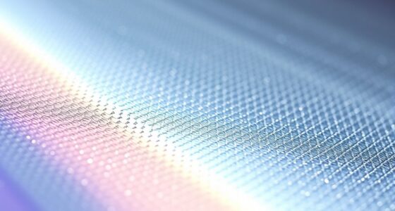
Have you ever wondered how extremely thin and uniform films are created at the atomic scale? Atomic Layer Deposition (ALD) achieves this by depositing materials one atomic layer at a time, ensuring exceptional layer uniformity. The process relies on sequential, self-limiting surface reactions that allow precise control over film thickness and composition. Because each reaction saturates automatically, ALD produces highly consistent coatings, even on complex surfaces. This method’s design also supports process scalability, making it suitable for large-area applications without sacrificing film quality. As a result, ALD is ideal for industries demanding meticulous nanostructures and coatings. Its ability to maintain uniformity at such a small scale, combined with scalable production, underscores its essential role in advanced nanofabrication. Additionally, the use of top materials like metal oxides and nitrides enhances the versatility of ALD processes across various technological fields.
Nanostructured Thin Film Deposition by Sputtering: From Fundamentals to Applications (Woodhead Publishing Reviews: Mechanical Engineering Series)
As an affiliate, we earn on qualifying purchases.
As an affiliate, we earn on qualifying purchases.
The ALD Process: Step-by-Step Overview

The ALD process unfolds through a series of carefully controlled, sequential steps that build up the film one atomic layer at a time. You cycle through precursor exposure, surface reactions, and purge steps, guaranteeing precise layer control and uniformity. This method assures excellent layer uniformity across complex surfaces and high process scalability for different substrate sizes. Additionally, the process’s inherent safety features contribute to its reliability in various applications. This step-by-step approach ensures consistent film quality, essential for nanofabrication applications.
metal oxide ALD precursors
As an affiliate, we earn on qualifying purchases.
As an affiliate, we earn on qualifying purchases.
Materials and Precursors Used in ALD

Choosing the right materials is essential for successful ALD processes, as they determine the quality and properties of the deposited films. You’ll find a variety of common precursors designed for different applications, but safety and handling are critical considerations. Understanding these factors helps guarantee efficient, safe, and high-quality nanofabrication. Additionally, knowledge of regional legal resources can assist in ensuring compliance with safety regulations and standards.
Materials Selection for ALD
What factors influence the selection of materials and precursors in atomic layer deposition (ALD)? Your choice depends heavily on substrate compatibility, ensuring that the material bonds well without damaging the surface. Precursors must have suitable volatility; they need to vaporize easily at deposition temperatures without decomposing. You also consider reactivity, ensuring the precursor reacts selectively and completely during each cycle. Stability is essential, so precursors don’t decompose prematurely. Cost and availability play roles, especially for large-scale processes. Compatibility with the process environment, such as temperature limits and inert atmospheres, guides your selection. Ultimately, you want materials that produce uniform, high-quality films while minimizing contamination, ensuring your ALD process is efficient and reliable.
Common Precursors in ALD
In atomic layer deposition, selecting the right precursors is key to achieving high-quality films. You’ll find that common precursors include organic precursors, which often contain carbon-based molecules that facilitate surface reactions, and metal halides, which supply metal ions essential for film growth. Organic precursors, such as alkyls and amides, are valued for their volatility and reactivity. Metal halides, like titanium tetrachloride (TiCl₄) or tungsten hexafluoride (WF₆), are frequently used for depositing metal oxides and nitrides. These precursors must be compatible with the ALD process, providing consistent, controlled reactions without unwanted byproducts. Understanding the properties of these materials allows you to optimize film quality, uniformity, and deposition efficiency in your nanofabrication projects.
Precursor Safety and Handling
Handling precursors safely is crucial to prevent health hazards and guarantee process stability in ALD. Many precursors have high precursor toxicity, making safe handling critical. Proper storage, ventilation, and protective gear minimize exposure risks. You should always work with fume hoods and gloves when handling volatile or toxic materials. Be aware that some precursors can decompose or react unexpectedly, so follow manufacturer guidelines carefully. Regular training ensures safe procedures and awareness of potential hazards. Proper disposal of residuals and contaminated materials is also indispensable to avoid environmental and health issues. Remember, understanding the specific properties of each precursor helps you implement effective safety measures. Prioritizing safe handling maintains both your safety and the integrity of your nanofabrication process.
- Use appropriate protective equipment
- Store precursors in designated areas
- Follow safety data sheets strictly
- Regularly train on handling procedures

Semiconductor Manufacturing for the AI Era
As an affiliate, we earn on qualifying purchases.
As an affiliate, we earn on qualifying purchases.
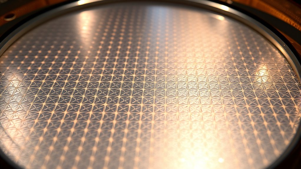
Applications of Nanofabrication With ALD

Atomic Layer Deposition enables you to create flexible electronics with precise control over thin films. You can also achieve high-precision coatings that enhance device performance and durability. These applications showcase ALD’s potential to revolutionize nanofabrication across industries. Additionally, understanding the health implications of nanomaterials is crucial for developing safe and sustainable technologies.
Flexible Electronics Integration
Flexible electronics have gained significant attention due to their potential to revolutionize wearable devices, sensors, and foldable displays. Atomic Layer Deposition (ALD) enables the precise fabrication of ultra-thin, conformal coatings on flexible substrates. This technique enhances substrate flexibility while maintaining device performance and durability. With ALD, you can integrate nanoscale films directly onto bendable surfaces, improving electrical properties and barrier protection. This supports seamless device integration without compromising flexibility. The key advantages include:
- Conformal coatings on complex geometries
- Enhanced mechanical stability
- Precise thickness control
- Compatibility with various flexible substrates
High-Precision Coatings
High-precision coatings created through ALD enable nanofabrication to achieve exceptional control over film thickness and uniformity. This precision guarantees strong interfacial adhesion, which is crucial for durable, high-performance devices. By carefully managing surface roughness, ALD produces smooth, defect-free coatings that enhance overall functionality. You’ll find that such coatings are ideal for applications requiring tight control over layer properties, like in electronics or protective barriers. The atomic-level thickness control allows for tailored surfaces with minimal imperfections, reducing issues related to surface irregularities. As a result, you can reliably produce coatings that promote better adhesion, stability, and performance, especially in complex nanostructures where precision directly impacts device efficiency and longevity.
Advantages and Challenges of ALD Techniques

While Atomic Layer Deposition (ALD) offers remarkable control over thin-film growth at the atomic scale, it also presents certain challenges that can limit its widespread adoption. Scalability limitations hinder ALD’s use in large-area manufacturing, making it less practical for high-volume production. Environmental concerns arise due to the use of toxic precursors and waste byproducts, raising sustainability questions. Additionally, ALD processes tend to be slow compared to other methods, impacting throughput. Cost factors, including equipment and precursor expenses, can also be prohibitive. To address these challenges, focus on improving process efficiency and adopting greener precursors. Considerations like scalability and environmental impact are critical for expanding ALD’s industrial applications and ensuring sustainable nanofabrication practices. High-precision deposition is essential for advancing ALD technology and overcoming current limitations.
Future Perspectives in ALD-Driven Nanotechnology

Advancements in ALD technology are paving the way for innovative applications across nanotechnology, promising to overcome current limitations and open new possibilities. As you explore future prospects, expect quantum effects to become more controllable at the nanoscale, leading to breakthroughs in quantum computing and sensing. Nanoscale patterning will reach unprecedented precision, enabling intricate device architectures and complex nanostructures. These developments will catalyze new capabilities in electronics, energy, and biomedical fields. Imagine a future where you can engineer materials atom-by-atom, pushing boundaries beyond current limits. The table below illustrates potential breakthroughs and their emotional impact:
| Innovation | Impact | Emotion |
|---|---|---|
| Quantum effects control | Enhanced computational power | Excitement |
| Nanoscale patterning | Ultra-precise devices | Inspiration |
| 3D nanostructures | Advanced multifunctionality | Hope |
| Material customization | Tailored properties | Confidence |
| Sustainable nanofabrication | Eco-friendly manufacturing | Optimism |
A deeper understanding of atomic-scale processes will accelerate the development of next-generation nanomaterials and devices.
Frequently Asked Questions
How Does ALD Compare to Other Nanofabrication Techniques in Cost?
Atomic Layer Deposition (ALD) generally has a higher cost compared to other nanofabrication techniques due to its precise, layer-by-layer process and specialized equipment. However, it offers better control and uniformity, making it economically feasible for high-precision applications. You should consider the cost comparison in relation to your project’s requirements, as ALD’s benefits can outweigh its higher initial costs when accuracy and quality are critical.
Can ALD Be Scaled for Industrial Mass Production Efficiently?
Like building the Tower of Babel, scaling ALD for mass production faces hurdles. You can overcome these scalability challenges through process automation, which boosts consistency and throughput. While ALD’s precise layer control is advantageous, adapting it for large-scale industrial use requires optimizing equipment and reducing cycle times. With technological advances and automation, you can make ALD more efficient, paving the way for its broader industrial implementation.
What Environmental Impacts Are Associated With ALD Processes?
You should know that ALD processes can contribute to environmental pollution through the release of volatile organic compounds and other chemicals. They also consume significant resources, such as precursors and energy, which impacts sustainability. While ALD offers precise control, you need to take into account these environmental impacts, including waste management and reducing resource use, to minimize ecological footprints and ensure safer, more eco-friendly manufacturing practices.
Are There Limitations to the Types of Nanostructures ALD Can Produce?
Sure, ALD’s limited, like a gourmet chef restricted to just salt and pepper. Its material versatility is impressive but struggles with creating highly complex nanostructures. You might find it challenging to produce intricate 3D architectures or multi-material systems, which require more than just layer-by-layer perfection. So, if your dreams involve wild, elaborate nanostructures, ALD might leave you craving more, like a chef with only one spice.
How Does Substrate Temperature Influence ALD Film Quality?
You’ll find that substrate temperature markedly influences ALD film quality. When you increase the temperature, it promotes better surface reactions, leading to denser and more uniform films. However, if you raise it too high, it can cause film degradation or unwanted reactions. Optimizing substrate temperature ensures you get high-quality, conformal coatings with controlled thickness, improving overall device performance and reliability.
Conclusion
By mastering the fundamentals, understanding the process, exploring materials, and recognizing applications, you can harness ALD’s potential. Embrace its advantages to innovate, address its challenges to improve, and envision its future to push nanofabrication boundaries. With precision, patience, and persistence, you can contribute to the evolving landscape of ALD-driven nanotechnology, shaping a future where materials are crafted atom by atom, and possibilities expand infinitely through meticulous layering and advanced fabrication techniques.