
Nanophotonics is driving faster internet by using tiny, high-speed optical components that control light at subwavelength scales. This lets you transfer data at rates exceeding 100 Gbit/s, with high efficiency and low energy use. Materials like graphene and plasmonic metals help create ultra-compact modulators and detectors, boosting network capacity through multiplexing. If you’re curious about how these innovations are transforming online speeds, there’s more to explore below.
Key Takeaways
- Nanophotonics enables ultra-compact, high-speed optical components supporting data transfer rates exceeding 100 Gbit/s.
- Advanced nanomaterials like graphene and metasurfaces facilitate rapid modulation and high-capacity data encoding.
- Integration of nanostructures reduces signal loss and latency in photonic circuits, boosting internet speed and efficiency.
- Multiplexing techniques such as DWDM expand bandwidth, accommodating growing data demands for faster connectivity.
- Nanophotonics advances support scalable, energy-efficient, and secure high-speed networks essential for next-generation internet infrastructure.

Homey Bridge | Smart Home Hub for Home Automation. Features Z-Wave Plus, Zigbee, Wi-Fi, BLE & Infrared. Compatible with Amazon Alexa & Google Home.
YOUR HOME, YOUR RULES: Make all your devices work together seamlessly with Homey Automatically play music when you...
As an affiliate, we earn on qualifying purchases.
Harnessing Nanophotonics for Next-Generation Data Transmission

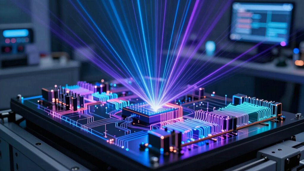
How can nanophotonics revolutionize data transmission? By enabling control of light at scales smaller than its wavelength, nanophotonics allows you to dramatically boost speed and efficiency. You can harness surface plasmon polaritons and nanostructures to confine electromagnetic fields tightly, supporting ultra-compact, high-bandwidth components. This technology makes it possible to transfer data at rates exceeding 100 Gbit/s per channel, with some systems approaching 400 Gbit/s. Energy consumption drops markedly too, with bits transmitted using less than 50 femtojoules. On-chip photonic routing shortens electrical traces, reducing losses and latency. Combining mode- and wavelength-multiplexing strategies further increases capacity. Additionally, nanoscale light manipulation enables unprecedented levels of integration and performance in photonic devices. All these advances mean faster, more efficient data links that can seamlessly integrate with existing infrastructure, transforming how data moves across networks. Innovative European Cloud Servers are leveraging these advancements to develop sustainable and secure cloud solutions.

Hubitat Elevation C-8 Pro Smart Home Hub - Local Control & Automation for Smart Thermostat, Voice Assistants, Ring Cameras - Compatible with Z-Wave 800 LR, Zigbee 3.0, Matter 1.5, Bluetooth, Wi-Fi
POWERFUL SMART HOME PERFORMANCE - EVEN WITHOUT INTERNET Hubitat C-8 Pro runs automations inside your home instead of...
As an affiliate, we earn on qualifying purchases.
Key Materials and Devices Powering Ultrafast Optical Communications

You can leverage advanced nanomaterials like graphene and plasmonic metals to create ultra-compact, high-speed modulators and detectors. These materials enable strong light–matter interactions, leading to faster switching speeds and lower energy consumption. Incorporating such devices into photonic circuits paves the way for ultrafast, energy-efficient optical communication systems. This integration of materials allows for the miniaturization and improved performance of photonic components, which is essential for next-generation networks. Additionally, optimizing contrast ratio and color accuracy in these systems can further enhance data transmission quality and reliability. The use of Free Floating structures can also facilitate innovative designs that improve device performance and integration. Integrating encryption techniques into photonic systems can also help secure high-speed data transfer against cyber threats.
Advanced Nanomaterials for Modulation
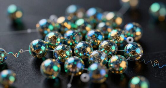
Advanced nanomaterials are transforming optical modulation by enabling ultrafast, energy-efficient control of light at the nanoscale. You leverage materials like graphene, which offers tunable conductivity and supports rapid modulation at terahertz speeds. Plasmonic metals such as gold and silver concentrate electromagnetic fields, allowing ultra-compact modulators with high bandwidths, though with some trade-offs in loss. Engineered dielectrics and metasurfaces enable flat optics and multifunctional devices, enhancing modulation capabilities without bulky components. You also utilize layered 2D materials like hBN for low-loss, high-speed modulation and single-photon emission. These advanced nanomaterials permit new levels of performance, reducing energy consumption while increasing data transfer speeds and device integration, essential for the next generation of ultrafast optical communication systems. optical modulation is further advanced by these innovative materials, paving the way for faster and more efficient data transmission technologies. Additionally, the integration of nanophotonic components enables precise control over light propagation and enhances overall system performance, with the development of ultrafast devices being a key focus of ongoing research. The unique properties of these materials also support energy-efficient systems, which are critical for sustainable technological progress. For example, the use of graphene-based modulators has shown promising results in achieving terahertz modulation speeds.
Ultra-Compact Photonic Devices
Nanophotonics leverages innovative materials and device architectures to create ultra-compact components capable of ultrafast optical data processing. You can harness silicon photonics to develop low-loss waveguides and integrated modulators that fit onto tiny chips, enabling high-speed data transfer. Plasmonic metals like gold and silver support subwavelength confinement, making devices smaller and more efficient, despite higher losses. 2D materials such as graphene offer ultrafast modulation and tunability, essential for high-throughput systems. Metasurfaces and nanostructured dielectrics shape beams and manage dispersion in compact forms. Nanoantennas and nanolasers push the limits of size and speed. These ultra-compact devices, combined with advanced fabrication, drive the miniaturization and speed of optical communication networks, paving the way for faster, more efficient internet infrastructure. Additionally, sustainable materials are increasingly being integrated into device fabrication to reduce environmental impact.

Philips Hue Bridge Pro, Smart Lighting Hub, Wireless, Advanced Encryption, Supports 150+ Lights & 50+ Accessories, Hue Bridge System Works with Apple Home, Alexa, Google, Samsung SmartThings
MORE SPEED: The Hue Bridge Pro features the Hue Chip Pro with ultra-fast processing speeds of 1.7 GHz...
As an affiliate, we earn on qualifying purchases.
Integration Strategies for Seamless Photonic and Electronic Systems

Integrating photonic and electronic systems seamlessly requires carefully designed strategies that bridge the different physical and operational characteristics of these domains. You need to focus on compatibility, minimizing losses, and guaranteeing efficient signal transfer. Silicon photonics plays a critical role by enabling CMOS-compatible fabrication, simplifying integration into existing semiconductor processes. Hybrid approaches combine electronic logic with photonic interconnects, reducing cabling and power consumption. Modular PICs can replace bulky copper links within servers, streamlining data flow. Overcoming packaging challenges, optimizing fiber-to-chip coupling, and managing heat are essential steps. To succeed, you must prioritize standardization, develop low-loss interconnects, and improve fabrication yields. These strategies ensure you create high-performance, scalable, and reliable integrated systems for faster internet infrastructure.

Lutron Caseta Smart Lighting Smart Hub for Light Bulbs and Fans, Compatible w/ Amazon Alexa, Apple Homekit, Google Home, 75 Device Capacity, L-BDG2-WH, White
CONNECTS WITH MORE LEADING SMART HOME BRANDS THAN ANY OTHER SMART HOME BRAND: Including Amazon Alexa, Apple HomeKit,...
As an affiliate, we earn on qualifying purchases.
Enhancing Network Capacity With Multiplexing and Nanostructures

Multiplexing techniques and nanostructures are at the forefront of boosting network capacity beyond traditional limits. You can leverage dense wavelength-division multiplexing (DWDM) to transmit multiple signals over a single fiber, markedly increasing bandwidth. Mode multiplexing at the nanoscale further multiplies data channels within compact devices. Nanostructures like plasmonic and dielectric elements confine light beyond diffraction limits, enabling ultra-compact components that support faster modulation and low-energy switching. Surface plasmon polaritons concentrate electromagnetic fields, boosting signal strength and enabling subwavelength routing. Photonic integrated circuits combine these nanostructures with waveguides, allowing you to process and route high-capacity data efficiently on-chip. Together, these advancements push the boundaries of network capacity, paving the way for faster, more reliable internet infrastructure.
Overcoming Challenges in Fabrication and System-Level Implementation

Despite the promising capabilities of nanophotonic systems, realizing their full potential hinges on overcoming significant fabrication and integration challenges. Achieving precise control at the nanoscale requires advanced manufacturing techniques, which often face low yields and high costs. Exploring advanced manufacturing techniques can help improve fabrication precision and yield, paving the way for scalable nanophotonics integration. Developing precise control at the nanoscale is essential to optimize system performance and ensure reliable operation in practical applications. Additionally, addressing system-level integration challenges is crucial for seamless deployment of nanophotonics in real-world communication networks. Incorporating appliance maintenance plans and ensuring compatibility with existing systems will be vital for integrating nanophotonics into current infrastructure and reducing operational costs. Moreover, establishing standardized fabrication protocols can significantly enhance consistency and scalability across different manufacturing facilities.
Real-World Applications Transforming Internet Infrastructure

You can see nanophotonics revolutionizing internet infrastructure through faster, more efficient data center connections and next-generation wireless links. These advancements enable higher bandwidth and lower latency, meeting the growing demands of digital communication. As a result, you’ll experience more reliable, scalable networks capable of supporting future technologies. Safe and smart home power solutions are essential to ensure these complex systems operate reliably and securely. Additionally, precise light control provided by nanophotonics enhances the performance and security of optical communication systems.
Data Center Connectivity
How is nanophotonics revolutionizing data center connectivity? It boosts speed, reduces power consumption, and shrinks device sizes. You’ll see nanophotonic interconnects exceeding 100 Gbit/s per channel, with some reaching 400 Gbit/s. These links consume less energy—fewer femtojoules per bit—compared to electronic options. Faster modulators and nanolasers improve latency and throughput, while on-chip routing minimizes electrical losses. Dense wavelength-division multiplexing (DWDM) and mode-multiplexing increase capacity within narrow spaces. You’ll also benefit from silicon photonics integration, enabling CMOS-compatible manufacturing for seamless system upgrades. Hybrid electronic-photonic processors and modular PICs simplify cabling and enhance scalability. Additionally, integrated photonic components are advancing the miniaturization and efficiency of these systems. As the field advances, photonic integration techniques are crucial for scaling these technologies to meet future demands. Moreover, innovations in nanofabrication methods are enabling the development of increasingly sophisticated photonic devices. These advances are complemented by ongoing research into material sciences to improve device performance and durability. Furthermore, ongoing developments in thermal management are essential to maintaining optimal operation of dense photonic systems. Overall, nanophotonics transforms data center infrastructure into faster, more efficient, and compact networks, supporting the growing demands of internet and cloud services.
Next-Gen Wireless Links
Nanophotonics is rapidly advancing wireless communication by enabling ultra-fast, high-capacity links for internet infrastructure. You can now leverage nanophotonic devices like nanoantennas and plasmonic modulators to achieve high-speed, short-range wireless connections with minimal latency. These technologies enable compact, tunable transceivers that support low-power operation while maintaining broad bandwidths essential for 5G, 6G, and IoT applications. By integrating nanophotonics into wireless systems, you improve data throughput and spectral efficiency, especially in dense urban environments. This allows for seamless, high-speed data transfer across devices, sensors, and edge nodes. As a result, nanophotonics transforms wireless links from bulky, power-hungry systems into streamlined, high-performance components, paving the way for faster, more reliable internet connectivity worldwide.
Future Directions and Innovations in Nanophotonic Technologies

Advances in nanophotonic technologies are poised to revolutionize the way you process and transmit data by pushing the boundaries of integration, efficiency, and functionality. Future innovations focus on developing ultra-compact, low-loss components that surpass current limits. Researchers are exploring new materials like 2D materials, metasurfaces, and hybrid systems to enhance tunability and speed. Integration with existing silicon platforms will streamline manufacturing and deployment, enabling seamless adoption. Efforts are also underway to improve fabrication techniques for higher yield and lower costs. Additionally, system-level co-design will optimize performance and interoperability across networks. These innovations promise to make your data systems faster, more efficient, and adaptable, *disclose* new possibilities for the future of high-speed internet and communications. Development of novel materials for enhanced performance can further accelerate these advancements by enabling more versatile and robust photonic devices.
Frequently Asked Questions
How Do Nanophotonic Devices Compare in Durability to Traditional Electronic Components?
Nanophotonic devices generally have comparable durability to traditional electronic components, but their longevity depends on materials and manufacturing quality. You might find that silicon photonics and 2D material modulators withstand operational stresses well, while plasmonic metals can degrade faster due to higher losses and thermal effects. Proper packaging, thermal management, and material choice are essential. With good design, nanophotonic devices can offer reliable, long-term performance similar to or exceeding that of electronic parts.
What Are the Environmental Impacts of Manufacturing Nanophotonic Systems at Scale?
You might picture a vast, shimmering factory floor where tiny materials are transformed into nanophotonic systems, but this process can have significant environmental impacts. Manufacturing at scale consumes energy, often from fossil fuels, releasing greenhouse gases. It also uses rare, sometimes toxic, materials that can pollute water and soil if not managed carefully. To minimize harm, adopting greener fabrication methods and recycling materials becomes essential as you expand nanophotonics.
How Secure Are Nanophotonics-Based Data Transmission Channels Against Cyber Threats?
You can rely on nanophotonics-based data channels for high security because they use light to transmit data, making eavesdropping much more difficult than with traditional electronic methods. Their rapid, wavelength-specific signals and advanced encryption add further protection. However, no system is completely immune, so you should stay aware of potential vulnerabilities like physical access or sophisticated cyber attacks, and implement layered security measures for maximum safety.
Can Current Fabrication Techniques Produce Defect-Free Nanostructures Reliably?
You might think producing defect-free nanostructures is a tall order, but current fabrication techniques have come a long way. Advanced methods like electron-beam lithography and atomic layer deposition enable high precision, consistently pushing the envelope. While perfect structures are challenging, ongoing improvements are steadily closing the gap. With ongoing research, you’ll find that reliable, high-quality nanostructures are becoming increasingly feasible, bringing nanophotonics closer to practical, large-scale applications.
What Is the Expected Timeline for Widespread Commercial Adoption of Nanophotonics?
You can expect widespread commercial adoption of nanophotonics within the next 5 to 10 years. As fabrication techniques improve, costs decrease, and industry standards emerge, integrating nanophotonics into data centers, telecom infrastructure, and consumer devices will accelerate. Ongoing research addresses current challenges like losses and thermal management, paving the way for faster, more efficient networks. However, full deployment depends on scaling production and overcoming remaining technical hurdles.
Conclusion
As you explore nanophotonics, remember it’s the lighthouse guiding your journey toward faster, more efficient internet. With innovations in materials, integration, and multiplexing, you’re on the brink of a technological leap. Challenges may loom like storms on the horizon, but your determination can turn them into stepping stones. Embrace this luminous future, for nanophotonics isn’t just a beacon—it’s the dawn illuminating the path to a connected world that’s brighter and boundless.